-
Product Categories
Live Support Chat


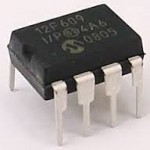
Unlock IC PIC12HV615 Heximal
Unlock IC PIC12HV615 flash and eeprom memory and extract IC code out from it, the file will be presented in the format of Heximal and replicate the content into other blank Microcontroller which will provide the same functions as original version;
Unlock IC PIC12HV615 flash and eeprom memory and extract IC code out from it, the file will be presented in the format of Heximal and replicate the content into other blank Microcontroller which will provide the same functions as original version
To read a program memory location, the user must write two bytes of the address to the PMADRL and PMADRH registers, and then set control bit RD (PMCON1<0>). Once the read control bit is set, the program memory Flash controller will use the second instruction cycle after to read the data.
This causes the second instruction immediately following the “BSF PMCON1,RD” instruction to be ignored. The data is available in the very next cycle in the PMDATL and PMDATH registers; it can be read as two bytes in the following instructions.
PMDATL and PMDATH registers will hold this value until another read or until it is written to by the user (during a write operation). A word of the Flash program memory may only be written to if the word is in an unprotected segment of memory after crack IC pic16c771 firmware.
Flash program memory must be written in four-word blocks. See Figure 3-2 and Figure 3-3 for more details. A block consists of four words with sequential addresses, with a lower boundary defined by an address, where PMADRL<1:0> = 00. All block writes to program memory are done as 16-word erase by four-word write operations.
The write operation is edge aligned and cannot occur across boundaries. To write program data, it must first be loaded into the buffer registers (see Figure 3-2). This is accomplished by first writing the destination address to PMADRL and PMADRH and then writing the data to PMDATL and PMDATH when crack mcu pic16c712 bin.
After the address and data have been set up, then the following sequence of events must be executed:
Write 55h, then AAh, to PMCON2 (Flash programming sequence). Set the WR control bit of the PMCON1 register. All four buffer register locations should be written to with correct data. If less than four words are being written to in the block of four words, then a read from the program memory location(s) not being written to must be performed.
This takes the data from the program location(s) not being written and loads it into the PMDATL and PMDATH registers. Then the sequence of events to transfer data to the buffer registers must be executed.
To transfer data from the buffer registers to the program memory, the PMADRL and PMADRH must point to the last location in the four-word block (PMADRL<1:0> = 11). Then the following sequence of events must be executed:
Write 55h, then AAh, to PMCON2 (Flash programming sequence). Set control bit WR of the PMCON1 register to begin the write operation.
The user must follow the same specific sequence to initiate the write for each word in the program block, writing each program word in sequence (000, 001, 010, 011). When the write is performed on the last word (PMADRL<1:0> = 11), a block of sixteen words is automatically erased and the content of the four-word buffer registers are written into the program memory.
After the “BSF PMCON1,WR” instruction, the processor requires two cycles to set up the erase/write operation. The user must place two NOP instructions after the WR bit is set. Since data is being written to buffer registers, the writing of the first three words of the block appears to occur immediately.
Tags: unlock ic binary archive,unlock ic binary code,unlock ic binary content,unlock ic binary data,unlock ic binary eeprom,unlock ic binary file,unlock ic binary firmware,unlock ic binary information,unlock ic binary memory,unlock ic binary program