-
Product Categories
Live Support Chat


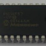
Unlock IC PIC10F204 Heximal
Unlock IC PIC10F204 secure memory and reset the security fuse bits from locked to unlocked, then readout the firmware in the format of Heximal.
Unlock IC PIC10F204 Heximal
The clock is internally divided by four to generate four non-overlapping quadrature clocks, namely Q1, Q2, Q3 and Q4. Internally, the PC is incremented every Q1 and the instruction is fetched from program memory and latched into the instruction register in Q4.
It is decoded and executed during the following Q1 through Q4. An instruction cycle consists of four Q cycles (Q1, Q2, Q3 and Q4). The instruction fetch and execute are pipelined such that fetch takes one instruction cycle, while decode and execute take another instruction cycle to carry out the Microcontroller copying. However, due to the pipelining, each instruction effectively executes in one cycle.
If an instruction causes the PC to change (e.g., GOTO), then two cycles are required to complete the instruction (Example 3-1). A fetch cycle begins with the PC incrementing in Q1. In the execution cycle, the fetched instruction is latched into the Instruction Register (IR) in cycle Q1. This instruction is then decoded and executed during the Q2, Q3 and Q4 cycles. Data memory is read during Q2 (operand read) and written during Q4 (destination write).
The PIC10F200/204 devices have a 9-bit Program Counter (PC) capable of addressing a 512 x 12 program memory space. Only the first 256 x 12 (0000h-00FFh) for the PIC10F200/204 are physically implemented (see Figure 4-1). Accessing a location above these boundaries will cause a wraparound within the first 256 x 12 space (PIC10F200/204).
The effective Reset vector is at 0000h (see Figure 4-1). Location 00FFh (PIC10F200/204) contains the internal clock oscillator calibration value. This value should never be overwritten. The PIC10F202/206 devices have a 10-bit Program Counter (PC) capable of addressing a 1024 x 12 program memory space.
Only the first 512 x 12 (0000h-01FFh) for the PIC10F202/206 are physically implemented (see Figure 4-2). Accessing a location above these boundaries will cause a wraparound within the first 512 x 12 space (PIC10F202/206). The effective Reset vector is at 0000h (see Figure 4-2). Location 01FFh (PIC10F202/206) contains the internal clock oscillator calibration value. This value should never be overwritten.
Data memory is composed of registers or bytes of RAM. Therefore, data memory for a device is specified by its register file. The register file is divided into two functional groups: Special Function Registers (SFR) and General Purpose Registers (GPR).
The Special Function Registers include the TMR0 register, the Program Counter (PCL), the STATUS register, the I/O register (GPIO) and the File Select Register (FSR). In addition, Special Function Registers are used to control the I/O port configuration and prescaler options.
Tags: unlock ic software archive,unlock ic software code,unlock ic software content,unlock ic software data,unlock ic software eeprom,unlock ic software file,unlock ic software firmware,unlock ic software information,unlock ic software memory,unlock ic software program