-
Product Categories
Live Support Chat


Unlock IC ATmeg1281A Heximal
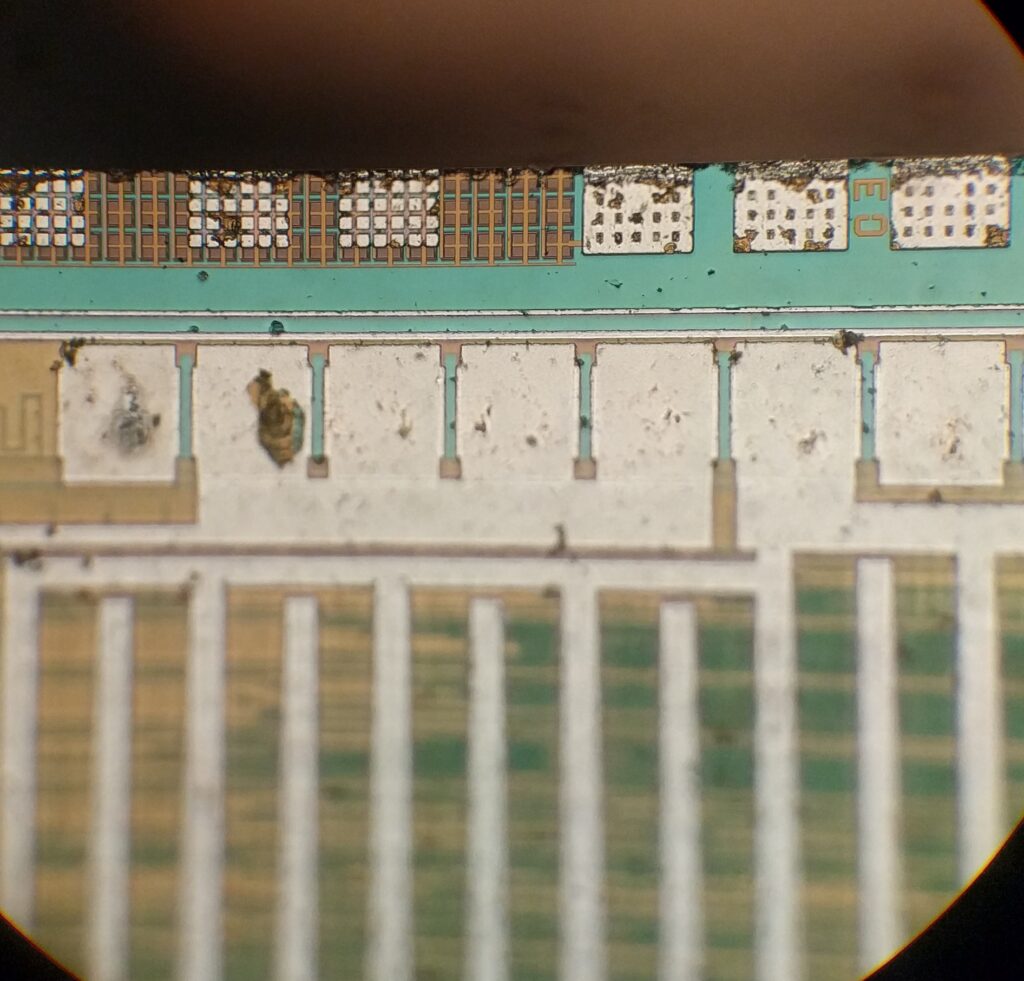
Unlock IC ATmeg1281A Heximal from its secured memory, breaking mcu atmega1281a fuse bit and then copy the program and data from microcontroller atmega1281a flash and eeprom memory;
The interconnection between master and slave CPUs with SPI is shown in the following figure. The SCK pin is the clock output in the master mode but is the clock input in the slave mode.
Writing to the SPI data register of the master CPU starts the SPI clock generator, and the data written shifts out of the MOSI pin and into the MOSI pin of the slave CPU. After shifting one byte, the SPI clock generator stops, setting the end of transmission flag (SPIF) if break mcu memory.
If both the SPI interrupt enable bit (SPIE) and the serial port interrupt enable bit (ES) are set, an interrupt is requested. The Slave Select input, SS/P1.4, is set low to select an individual SPI device as a slave. When SS/P1.4 is set high, the SPI port is deactivated and the MOSI/P1.5 pin can be used as an input.
There are four combinations of SCK phase and polarity with respect to serial data, which are determined by control bits CPHA and CPOL. The SPI data transfer formats are shown in Figures 8 and 9.
The AT89S53 has a total of six interrupt vectors: two external interrupts (INT0 and INT1), three timer interrupts (Timers 0, 1, and 2), and the serial port interrupt. These interrupts are all shown in Figure 10.
Each of these interrupt sources can be individually enabled or disabled by setting or clearing a bit in Special Function Register IE. IE also contains a global disable bit, EA, which disables all interrupts at once if unlock IC microcontroller heximal.
Note that Table 10 shows that bit position IE.6 is unimplemented. In the AT89C51, bit position IE.5 is also unimplemented. User software should not write 1s to these bit positions, since they may be used in future AT89 products.
Timer 2 interrupt is generated by the logical OR of bits TF2 and EXF2 in register T2CON. Neither of these flags is cleared by hardware when the service routine is vectored
- In fact, the service routine may have to determine whether it was TF2 or EXF2 that generated the interrupt, and that bit will have to be cleared in software.
The Timer 0 and Timer 1 flags, TF0 and TF1, are set at S5P2 of the cycle in which the timers overflow. The values are then polled by the circuitry in the next cycle. However, the Timer 2 flag, TF2, is set at S2P2 and is polled in the same cycle in which the timer overflows after unlock IC heximal.
Tags: unlock ic archive,unlock ic bin,unlock ic code,unlock ic content,unlock ic data,unlock ic eeprom,unlock ic file,unlock ic firmware,unlock ic hex,unlock ic information,unlock ic memory,unlock ic program
Related Products
-
Unlock IC Chip
No.