-
Product Categories
Live Support Chat


Unlock Chip PIC18F4525 Binary
Unlock Chip PIC18F4525 memory and extract the source code from memory include flash and eeprom in the format of binary or heximal, then download the firmware into blank Microcontroller to provide the same functions;
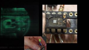
Unlock Chip PIC18F4525 memory and extract the source code from memory
Fail-Safe Clock Monitor: This option constantly monitors the main clock source against a reference signal provided by the internal oscillator. If a clock failure occurs, the controller is switched to the internal oscillator block, allowing for continued low-speed operation or a safe application shutdown.
· Two-Speed Start-up: This option allows the internal oscillator to serve as the clock source from Power-on Reset, or wake-up from Sleep mode, until the primary clock source is available.
· Memory Endurance: The Enhanced Flash cells for both program memory and data EEPROM are rated to last for many thousands of erase/write cycles – up to 100,000 for program memory and 1,000,000 for EEPROM. Data retention without refresh is conservatively estimated to be greater than 40 years.
· Self-Programmability: These devices can write to their own program memory spaces under internal software control. By using a bootloader routine located in the protected Boot Block at the top of program memory, it becomes possible to create an application that can update itself in the field.
· Extended Instruction Set: The PIC18F4525 family introduces an optional extension to the PIC18 instruction set, which adds 8 new instructions and an Indexed Addressing mode to facilitate the process of MCU Content reading. This extension, enabled as a device configuration option, has been specifically designed to optimize re-entrant application code originally developed in high-level languages, such as C.
Enhanced CCP Module: In PWM mode, this module provides 1, 2 or 4 modulated outputs for controlling half-bridge and full-bridge drivers. Other features include auto-shutdown, for disabling PWM outputs on interrupt or other select conditions and auto-restart, to reactivate outputs once the condition has cleared.
· Enhanced Addressable USART: This serial communication module is capable of standard RS-232 operation and provides support for the LIN bus protocol. Other enhancements include automatic baud rate detection and a 16-bit Baud Rate Generator for improved resolution. When the microcontroller is using the internal oscillator block, the EUSART provides stable operation for applications that talk to the outside world without using an external crystal (or its accompanying power requirement).
· 10-Bit A/D Converter: This module incorporates programmable acquisition time, allowing for a channel to be selected and a conversion to be initiated without waiting for a sampling period and thus, reducing code overhead.
Extended Watchdog Timer (WDT): This enhanced version incorporates a 16-bit prescaler, allowing an extended time-out range that is stable across operating voltage and temperature. See
Section 26.0 “Electrical Characteristics” for time-out periods.
Devices in the PIC18F4525 family are available in 28-pin and 40/44-pin packages. Block diagrams for the two groups are shown in Figure 1-1 and Figure 1-2.
The devices are differentiated from each other in five ways:
1. Flash program memory (48 Kbytes for PIC18FX525 devices, 64 Kbytes for PIC18FX620 devices).
A/D channels (10 for 28-pin devices, 13 for 40/44-pin devices). I/O ports (3 bidirectional ports on 28-pin devices,
5 bidirectional ports on 40/44-pin devices). CCP and Enhanced CCP implementation (28-pin devices have 2 standard CCP modules, 40/44-pin devices have one standard CCP module and one ECCP module).
Parallel Slave Port (present only on 40/44-pin devices).
All other features for devices in this family are identical. These are summarized in Table 1-1. The pinouts for all devices are listed in Table 1-2 and Table 1-3.
Like all Microchip PIC18 devices, members of the PIC18F4525 family are available as both standard and low-voltage devices. Standard devices with Enhanced Flash memory, designated with an “F” in the part number (such as PIC18F2620), accommodate an operating VDD range of 4.2V to 5.5V if Unlock Chip.
Low-voltage parts, designated by “LF” (such as PIC18LF2620), function over an extended VDD range of 2.0V to 5.5V.
Tags: unlock chip encrypted archive,unlock chip encrypted code,unlock chip encrypted content,unlock chip encrypted data,unlock chip encrypted eeprom,unlock chip encrypted file,unlock chip encrypted firmware,unlock chip encrypted information,unlock chip encrypted memory,unlock chip encrypted program