-
Product Categories
Live Support Chat


Unlock Chip PIC18F4320 Heximal
Unlock Chip PIC18F4320 Heximal and recover the content from its flash and eeprom memory, engineer will locate the security fuse bits of Microcontroller then disable it by using focus ion beam to cut it off;
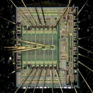
Unlock Chip PIC18F4320 Heximal and recover the content from its flash and eeprom memory, engineer will locate the security fuse bits of Microcontroller then disable it by using focus ion beam to cut it off
The EC and ECIO Oscillator modes require an external clock source to be connected to the OSC1 pin. There is no oscillator start-up time required after a Power-on Reset or after an exit from Sleep mode.
In the EC Oscillator mode, the oscillator frequency divided by 4 is available on the OSC2 pin. This signal may be used for test purposes or to synchronize other logic. Figure 2-4 shows the pin connections for the EC Oscillator mode.
For timing insensitive applications, the “RC” and “RCIO” device options offer additional cost savings. The RC oscillator frequency is a function of the supply voltage, the resistor (REXT) and capacitor (CEXT) values and the operating temperature. In addition to this, the oscillator frequency will vary from unit to unit due to normal manufacturing variation before extract chip pic16hv785 hex.
Furthermore, the difference in lead frame capacitance between package types will also affect the oscillation frequency, especially for low CEXT values. The user also needs to take into account variation due to tolerance of external R and C components used. Figure 2-6 shows how the R/C combination is connected.
In the RC Oscillator mode, the oscillator frequency divided by 4 is available on the OSC2 pin. This signal may be used for test purposes or to synchronize other logic.
A Power-on Reset pulse is generated on-chip when VDD rise is detected. To take advantage of the POR circuitry, just tie the MCLR pin through a resistor (1k to 10 kΩ) to VDD. This will eliminate external RC components usually needed to create a Power-on Reset delay.
A minimum rise rate for VDD is specified (parameter D004). For a slow rise time, see Figure 4-2. When the device starts normal operation (i.e., exits the Reset condition), device operating parameters (voltage, frequency, temperature, etc.) must be met to ensure successful operation of Microcontroller copying.
If these conditions are not met, the device must be held in Reset until the operating conditions are met. The Oscillator Start-up Timer (OST) provides a 1024 oscillator cycle (from OSC1 input) delay after the PWRT delay is over (parameter #33). This ensures that the crystal oscillator or resonator has started and stabilized.
The OST time-out is invoked only for XT, LP, HS and HSPLL modes and only on Power-on Reset, or on exit from most power managed modes. With the PLL enabled in its PLL mode, the time-out sequence following a Power-on Reset is slightly different from other oscillator modes.
A portion of the Power-up Timer is used to provide a fixed time-out that is sufficient for the PLL to lock to the main oscillator frequency. This PLL lock time-out (TPLL) is typically 2 ms and follows the oscillator start-up time-out.
A configuration bit, BOREN, can disable (if clear/programmed) or enable (if set) the Brown-out Reset circuitry. If VDD falls below VBOR (parameter D005) for greater than TBOR (parameter #35), the brown-out situation will reset the chip. A Reset may not occur if VDD falls below VBOR for less than TBOR.
The chip will remain in Brown-out Reset until VDD rises above VBOR. If the Power-up Timer is enabled, it will be invoked after VDD rises above VBOR; it then will keep the chip in Reset for an additional time delay TPWRT (parameter #33). If VDD drops below VBOR while the Power-up Timer is running, the chip will go back into a Brown-out Reset and the Power-up Timer will be initialized. Once VDD rises above VBOR, the Power-up Timer will execute the additional time delay. Enabling BOR Reset does not automatically enable the PWRT. The Power-up Timer (PWRT) of the PIC18F2X20/4X20 devices is an 11-bit counter, which uses the INTRC source as the clock input. This yields a count of 2048 x 32 µs = 65.6 ms. While the PWRT is counting, the device is held in Reset.
The power-up time delay depends on the INTRC clock and will vary from chip-to-chip due to temperature and process variation. See DC parameter #33 for details. The PWRT is enabled by clearing configuration bit, PWRTEN.
Tags: адамкнуць ic bin,адамкнуць Intergated замыкання firmware,адамкнуць mcu hex,адамкнуць мікракантролер program,адамкнуць чып code,чытаць ic archive,чытаць Intergated замыкання flash,чытаць mcu dump,чытаць мікракантролер eeprom,чытаць чып content