-
Product Categories
Live Support Chat


Unlock Chip ATMEGA88P Program
Unlock Chip ATMEGA88P flash and eeprom memory and extract IC program out from the locked Microcontroller ATmega88P after disable the security fuse bit by crack MCU protective system;
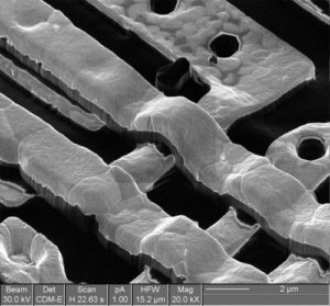
Unlock Chip ATMEGA88P flash and eeprom memory and extract IC program out from the locked Microcontroller ATmega88P after disable the security fuse bit by crack MCU protective system
The interrupt execution response for all the enabled AVR interrupts is four clock cycles minimum. After four clock cycles the program vector address for the actual interrupt handling routine is executed. During this four clock cycle period, the Program Counter is pushed onto the Stack.
The vector is normally a jump to the interrupt routine, and this jump takes three clock cycles. If an interrupt occurs during execution of a multi-cycle instruction, this instruction is completed before the interrupt is served. If an interrupt occurs when the MCU is in sleep mode, the interrupt execution response time is increased by four clock cycles if Unlock microcontroller ATmega8535L code .
This increase comes in addition to the start-up time from the selected sleep mode. A return from an interrupt handling routine takes four clock cycles. During these four clock cycles, the Program Counter (two bytes) is popped back from the Stack, the Stack Pointer is incremented by two, and the I-bit in SREG is set.
The ATmega48/88/168 contains 4/8/16K bytes On-chip In-System Reprogrammable Flash memory for program storage. Since all AVR instructions are 16 or 32 bits wide, the Flash is organized as 2/4/8K x 16. For software security, the Flash Program memory space is divided into two sections, Boot Loader Section and Application Program Section in ATmega88 and ATmega168 after Crack IC ATmega48 heximal.
ATmega48 does not have separate Boot Loader and Application Program sections, and the SPM instruction can be executed from the entire Flash. The Flash memory has an endurance of at least 10,000 write/erase cycles. The ATmega48/88/168 Program Counter (PC) is 11/12/13 bits wide, thus addressing the 2/4/8K program memory locations. The operation of Boot Program section and associated Boot Lock bits.
The ATmega48/88/168 is a complex microcontroller with more peripheral units than can be supported within the 64 locations reserved in the Opcode for the IN and OUT instructions. For the Extended I/O space from 0x60 – 0xFF in SRAM, only the ST/STS/STD and LD/LDS/LDD instructions can be used.
The lower 768/1280/1280 data memory locations address both the Register File, the I/O memory, Extended I/O memory, and the internal data SRAM. The first 32 locations address the Register File, the next 64 location the standard I/O memory, then 160 locations of Extended I/O memory, and the next 512/1024/1024 locations address the internal data SRAM.
The five different addressing modes for the data memory cover: Direct, Indirect with Displacement, Indirect, Indirect with Pre-decrement, and Indirect with Post-increment. In the Register File, registers R26 to R31 feature the indirect addressing pointer registers.
The direct addressing reaches the entire data space. The Indirect with Displacement mode reaches 63 address locations from the base address given by the Y- or Z-register. When using register indirect addressing modes with automatic pre-decrement and post-increment, the address registers X, Y, and Z are decremented or incremented. The 32 general purpose working registers, 64 I/O Registers, 160 Extended I/O Registers, and the 512/1024/1024 bytes of internal data SRAM in the ATmega48/88/168.
Tags: chip unlocking locked archive,chip unlocking locked binary,chip unlocking locked code,chip unlocking locked content,chip unlocking locked eeprom,chip unlocking locked file,chip unlocking locked firmware,chip unlocking locked heximal,chip unlocking locked information,chip unlocking locked memory,chip unlocking locked program