-
Product Categories
Live Support Chat


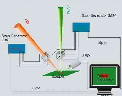
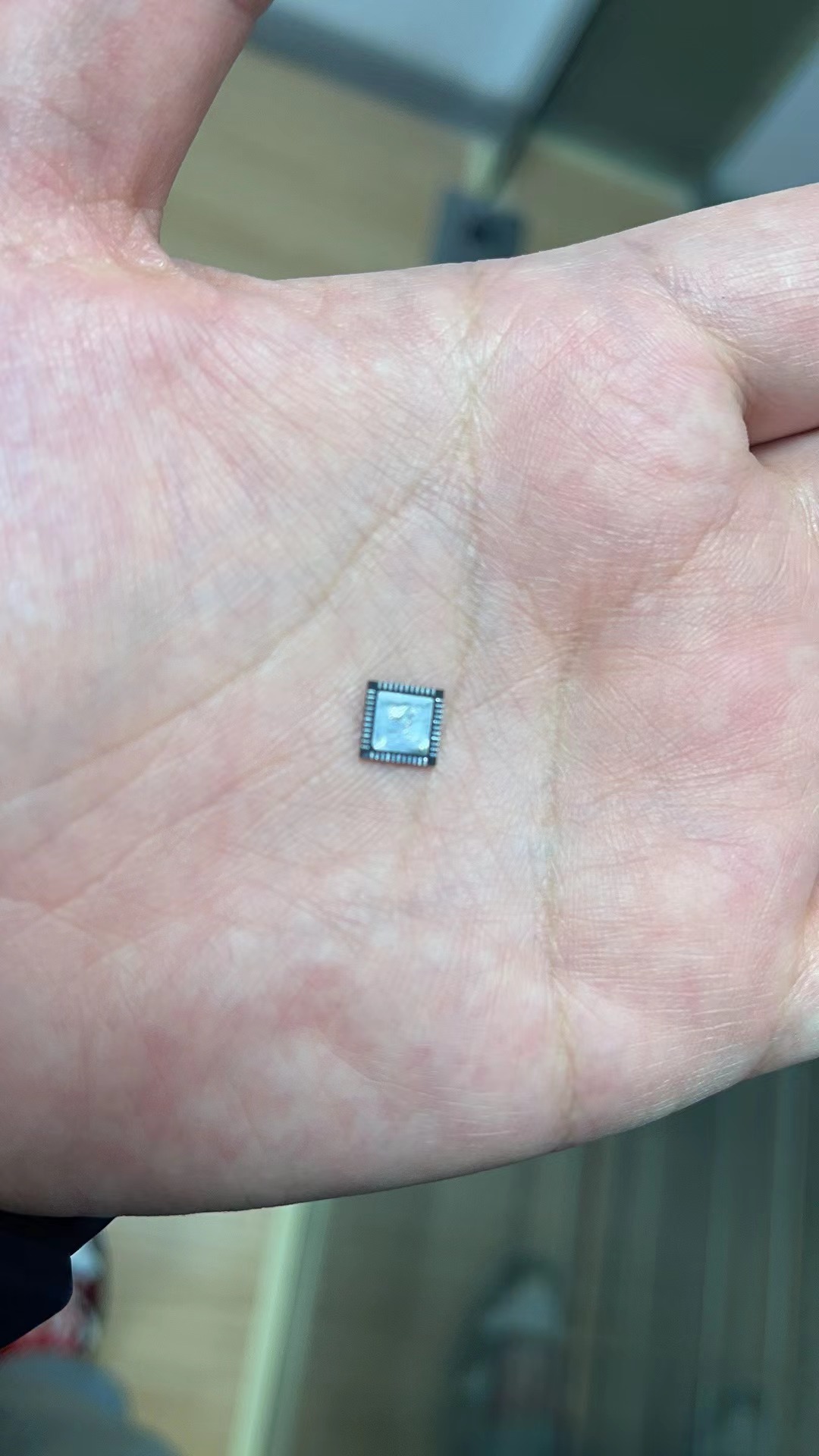
Unlock Chip ATmega1280V Flash
Unlock Chip ATmega1280V by using focus ion beam technique, readout mcu atmega1280v Flash program, and make microcontroller atmega1280v recovery as cloning.
To program and verify the AT89S53 in the parallel programming mode, the following sequence is recommended:
- Power-up sequence:
Apply power between VCC and GND pins.
Set RST pin to “H”.
Apply a 3 MHz to 24 MHz clock to XTAL1 pin and wait for at least 10 milliseconds when crack pic16f616 chip heximal flash.
- Set PSEN pin to “L”
ALE pin to “H”
EA pin to “H” and all other pins to “H”.
- Apply the appropriate combination of “H” or “L” logic levels to pins P2.6, P2.7, P3.6, P3.7 to select one of the programming operations shown in the Flash Programming Modes table.
- Apply the desired byte address to pins P1.0 to P1.7 and P2.0 to P2.5.
Apply data to pins P0.0 to P0.7 for Write Code operation.
- Raise EA/VPP to 12V to enable Flash programming, erase or verification.
- Pulse ALE/PROG once to program a byte in the Code memory array, or the lock bits. The byte-write cycle is self-timed and typically takes 1.5 ms before unlock pic12f609 chip heximal flash.
- To verify the byte just programmed, bring pin P2.7 to “L” and read the programmed data at pins P0.0 to P0.7.
- Repeat steps 3 through 7 changing the address and data for the entire 12K-byte array or until the end of the object file is reached.
- Power-off sequence:
Set XTAL1 to “L”.
Set RST and EA pins to “L”.
Turn VCC power off.
The AT89S53 features DATA Polling to indicate the end of a write cycle. During a write cycle in the parallel or serial programming mode, an attempted read of the last byte written will result in the complement of the written datum on P0.7 (parallel mode), and on the MSB of the serial output byte on MISO (serial mode) when extract pic12f636 chip flash code.
Once the write cycle has been completed, true data are valid on all outputs, and the next cycle may begin. DATA Polling may begin any time after a write cycle has been initiated.
The progress of byte programming in the parallel programming mode can also be monitored by the RDY/BSY output signal. Pin P3.4 is pulled Low after ALE goes High during programming to indicate BUSY. P3.4 is pulled High again when programming is done to indicate READY.