-
Product Categories
Live Support Chat


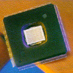
Unlock Chip AT89C51RC Binary
Unlock Chip AT89C51RC and extract Binary from microcontroller AT89C51RC flash memory, the content inside MCU will be recovered and copy to new Microprocessor;
The AT89C51RC is a low-power, high-performance CMOS 8-bit microcontroller with 32K bytes of Flash programmable read-only memory and 512 bytes of RAM. The device is manufactured using Atmel’s high-density nonvolatile memory technology and is compatible with the industry-standard 80C51 and 80C52 instruction set and pinout when extract mcu pic16cr84 code.
The on-chip Flash allows the program memory to be user programmed by a conventional nonvolatile memory programmer. A total of 512 bytes of internal RAM are available in the AT89C51RC.
The 256-byte expanded internal RAM is accessed via MOVX instructions after clearing bit 1 in the SFR located at address 8EH. The other 256-byte RAM segment is accessed the same way as the Atmel AT89-series and other 8052-compatible products if extract Chip pic16c554a eeprom.
By combining a versatile 8-bit CPU with Flash on a monolithic chip, the Atmel AT89C51RC is a powerful microcomputer which provides a highly-flexible and cost-effective solution to many embedded control applications.
The AT89C51RC provides the following standard features: 32K bytes of Flash, 512 bytes of RAM, 32 I/O lines, three 16-bit timer/counters, a six-vector two-level interrupt architecture, a full duplex serial port, on-chip oscillator, and clock circuitry before Unlock mcu pic16c558 program.
In addition, the AT89C51RC is designed with static logic for operation down to zero frequency and supports two software selectable power saving modes. The Idle Mode stops the CPU while allowing the RAM, timer/counters, serial port, and interrupt system to continue functioning.
The Power-down mode saves the RAM contents but freezes the oscillator, disabling all other chip functions until the next external interrupt or hardware reset.
Port 1 is an 8-bit bi-directional I/O port with internal pull-ups. The Port 1 output buffers can sink/source four TTL inputs. When 1s are written to Port 1 pins, they are pulled high by the internal pull-ups and can be used as inputs.
As inputs, Port 1 pins that are externally being pulled low will source current (IIL) because of the internal pull-ups. In addition, P1.0 and P1.1 can be configured to be the timer/counter 2 external count input (P1.0/T2) and the timer/counter 2 trigger input (P1.1/T2EX), respectively, as shown in the following table.
Port 2 is an 8-bit bi-directional I/O port with internal pull-ups. The Port 2 output buffers can sink/source four TTL inputs. When 1s are written to Port 2 pins, they are pulled high by the internal pull-ups and can be used as inputs. As inputs, Port 2 pins that are externally being pulled low will source current (IIL) because of the internal pull-ups.
Port 2 emits the high-order address byte during fetches from external program memory and during accesses to external data memory that use 16-bit addresses (MOVX @ DPTR). In this application, Port 2 uses strong internal pull-ups when emitting 1s.
During accesses to external data memory that use 8-bit addresses (MOVX @ RI), Port 2 emits the contents of the P2 Special Function Register. Port 2 also receives the high-order address bits and some control signals during Flash programming and verification.
Tags: unlock chip heximal archive,unlock chip heximal code,unlock chip heximal content,unlock chip heximal data,unlock chip heximal eeprom,unlock chip heximal file,unlock chip heximal firmware,unlock chip heximal information,unlock chip heximal memory,unlock chip heximal program
