-
Product Categories
Live Support Chat


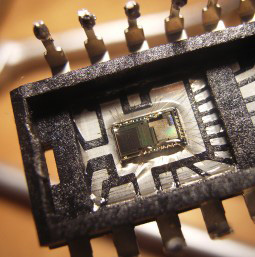
Reverse DSP IC Microcontroller Texas Instruments TMS320LF2401AVFA
Reverse DSP IC Microcontroller Texas Instruments TMS320LF2401AVFA
We can Reverse DSP IC Microcontroller Texas Instruments TMS320LF2401AVFA, please view below chip features for your reference:
High-Performance Static CMOS Technology
− 25-ns Instruction Cycle Time (40 MHz)
− 40-MIPS Performance
− Low-Power 3.3-V Design
Based on TMS320C2xx DSP CPU Core
− Code-Compatible With F243/F241/C242
− Instruction Set and Module Compatible With F240 Flash (LF) and ROM (LC) Device Options
− LF240xA: LF2407A, LF2406A, LF2403A, LF2402A
− LC240xA: LC2406A, LC2404A, LC2403A, LC2402A
On-Chip Memory
− Up to 32K Words x 16 Bits of Flash EEPROM (4 Sectors) or ROM
− Programmable “Code-Security” Feature for the On-Chip Flash/ROM
− Up to 2.5K Words x 16 Bits of Data/Program RAM
− 544 Words of Dual-Access RAM
− Up to 2K Words of Single-Access RAM Boot ROM (LF240xA Devices)
− SCI/SPI Bootloader
Up to Two Event-Manager (EV) Modules (EVA and EVB), Each Includes:
− Two 16-Bit General-Purpose Timers
− Eight 16-Bit Pulse-Width Modulation (PWM) Channels Which Enable:
− Three-Phase Inverter Control
− Center- or Edge-Alignment of PWM Channels
− Emergency PWM Channel Shutdown With External PDPINTx Pin
− Programmable Deadband (Deadtime) Prevents Shoot-Through Faults
− Three Capture Units for Time-Stamping of External Events
− Input Qualifier for Select Pins
− On-Chip Position Encoder Interface Circuitry
− Synchronized A-to-D Conversion
− Designed for AC Induction, BLDC, Switched Reluctance, and Stepper Motor Control
− Applicable for Multiple Motor and/or Converter Control
External Memory Interface (LF2407A)
− 192K Words x 16 Bits of Total Memory:
64K Program, 64K Data, 64K I/O
Watchdog (WD) Timer Module
10-Bit Analog-to-Digital Converter (ADC)
− 8 or 16 Multiplexed Input Channels
− Selectable Twin 8-State Sequencers
Triggered by Two Event Managers
Controller Area Network (CAN) 2.0B Module
(LF2407A, 2406A, 2403A)
Serial Communications Interface (SCI)
16-Bit Serial Peripheral Interface (SPI)
(LF2407A, 2406A, LC2404A, 2403A)
Phase-Locked-Loop (PLL)-Based Clock
Generation
Up to 40 Individually Programmable, Multiplexed General-Purpose Input / Output (GPIO) Pins
Up to Five External Interrupts (Power Drive Protection, Reset, Two Maskable Interrupts)
Power Management:
− Three Power-Down Modes
− Ability to Power Down Each Peripheral Independently
Real-Time JTAG-Compliant Scan-Based
Emulation, IEEE Standard 1149.1† (JTAG)
Development Tools Include:
− Texas Instruments (TI) ANSI C Compiler, Assembler/ Linker, and Code Composer Studio Debugger
− Evaluation Modules
− Scan-Based Self-Emulation (XDS510)
− Broad Third-Party Digital Motor Control Support
Package Options
− 144-Pin LQFP PGE (LF2407A)
− 100-Pin LQFP PZ (2406A, LC2404A)
− 64-Pin TQFP PAG (LF2403A, LC2403A, LC2402A)
− 64-Pin QFP PG (2402A)
Extended Temperature Options (A and S)
− A: − 40°C to 85°C
− S: − 40°C to 125°C