-
Product Categories
Live Support Chat


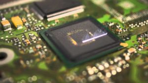
Read TI DSP IC TMS320LF2406APZAR Flash
We can read TI DSP IC TMS320LF2406APZAR Flash, below is the chip features for your reference:
High-Performance Static CMOS Technology
− 25-ns Instruction Cycle Time (40 MHz)
− 40-MIPS Performance
− Low-Power 3.3-V Design
D Based on TMS320C2xx DSP CPU Core
− Code-Compatible With F243/F241/C242
− Instruction Set and Module Compatible With F240 D Flash (LF) and ROM (LC) Device Options
− LF240xA: LF2407A, LF2406A, LF2403A, LF2402A
− LC240xA: LC2406A, LC2404A, LC2403A, LC2402A D On-Chip Memory
− Up to 32K Words x 16 Bits of Flash EEPROM (4 Sectors) or ROM
− Programmable “Code-Security” Feature for the On-Chip Flash/ROM
− Up to 2.5K Words x 16 Bits of Data/Program RAM
− 544 Words of Dual-Access RAM
− Up to 2K Words of Single-Access RAM D Boot ROM (LF240xA Devices)
− SCI/SPI Bootloader D Up to Two Event-Manager (EV) Modules (EVA and EVB), Each Includes:
− Two 16-Bit General-Purpose Timers
− Eight 16-Bit Pulse-Width Modulation (PWM) Channels Which Enable:
− Three-Phase Inverter Control
− Center- or Edge-Alignment of PWM Channels
− Emergency PWM Channel Shutdown With External PDPINTx Pin
− Programmable Deadband (Deadtime) Prevents Shoot-Through Faults
− Three Capture Units for Time-Stamping of External Events
− Input Qualifier for Select Pins
− On-Chip Position Encoder Interface Circuitry
− Synchronized A-to-D Conversion
− Designed for AC Induction, BLDC, Switched Reluctance, and Stepper Motor Control
− Applicable for Multiple Motor and/or Converter Control D External Memory Interface (LF2407A)
− 192K Words x 16 Bits of Total Memory:
64K Program, 64K Data, 64K I/O
D Watchdog (WD) Timer Module
D 10-Bit Analog-to-Digital Converter (ADC)
− 8 or 16 Multiplexed Input Channels
− 500-ns MIN Conversion Time
− Selectable Twin 8-State Sequencers Triggered by Two Event Managers
D Controller Area Network (CAN) 2.0B Module (LF2407A, 2406A, 2403A)
D Serial Communications Interface (SCI)
D 16-Bit Serial Peripheral Interface (SPI)
(LF2407A, 2406A, LC2404A, 2403A)
D Phase-Locked-Loop (PLL)-Based Clock Generation
D Up to 40 Individually Programmable,
Multiplexed General-Purpose Input / Output (GPIO) Pins
D Up to Five External Interrupts (Power Drive Protection, Reset, Two Maskable Interrupts)
D Power Management:
− Three Power-Down Modes
− Ability to Power Down Each Peripheral Independently
D Real-Time JTAG-Compliant Scan-Based Emulation, IEEE Standard 1149.1† (JTAG)
D Development Tools Include:
− Texas Instruments (TI) ANSI C Compiler,
Assembler/ Linker, and Code Composer
Studio Debugger
− Evaluation Modules
− Scan-Based Self-Emulation (XDS510)
− Broad Third-Party Digital Motor Control Support D Package Options
− 144-Pin LQFP PGE (LF2407A)
− 100-Pin LQFP PZ (2406A, LC2404A)
− 64-Pin TQFP PAG (LF2403A, LC2403A, LC2402A)
− 64-Pin QFP PG (2402A)