-
Product Categories
Live Support Chat


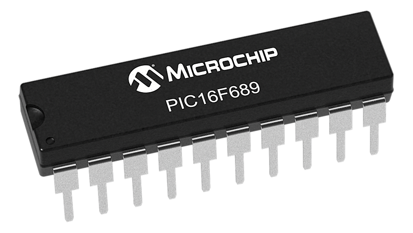
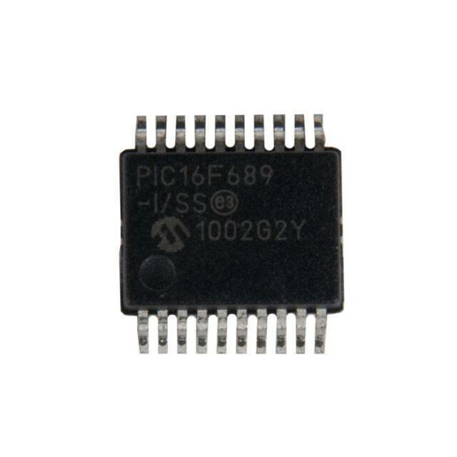
Read Microchip IC PIC16F689 Software
Read Microchip IC PIC16F689 program memory and extract the Software from microcontroller PIC16F689 embedded memory, the content of the MCU PIC16F689 can be recovered completely for MCU cloning;
The data memory (see Figures 2-6 through 2-8) is partitioned into four banks which contain the General Purpose Registers (GPR) and the Special Function Registers (SFR). The Special Function Registers are located in the first 32 locations of each bank. The General Purpose Registers, implemented as static RAM, are located in the last 96 locations of each Bank.
Register locations F0h-FFh in Bank 1, 170h-17Fh in Bank 2 and 1F0h-1FFh in Bank 3 point to addresses 70h-7Fh in Bank 0. The actual number of General Purpose Resisters (GPR) in each Bank depends on the device. Details are shown in Figures 2-4 through 2-8. All other RAM is unimplemented and returns ‘0’ when Reset Vector 0000h read. RP<1:0> of the STATUS register are the bank select bits:
The register file is organized as 128 x 8 in the PIC16F687 and 256 x 8 in the PIC16F685/PIC16F689/PIC16F690. Each register is accessed, either directly or indirectly, through the File Select Register (FSR) (see Section 2.4 “Indirect Addressing, INDF and FSR Registers”). SPECIAL FUNCTION REGISTERS after Read Microchip IC
The Special Function Registers are registers used by the CPU and peripheral functions for controlling the desired operation of the device (see Tables 2-1 through 2-4). These registers are static RAM.
The special registers can be classified into two sets: core and peripheral. The Special Function Registers associated with the “core” are described in this section. Registers related to the operation of peripheral features are described in the section of that peripheral feature.
The STATUS register, shown in Register 2-1, contains:
· the arithmetic status of the ALU
· the Reset status
· the bank select bits for data memory (GPR and SFR)
The STATUS register can be the destination for any instruction, like any other register. If the STATUS register is the destination for an instruction that affects the Z, DC or C bits, then the write to these three bits is disabled. These bits are set or cleared according to the device logic. Furthermore, the TO and PD bits are not writable. Therefore, the result of an instruction with the STATUS register as destination may be different than intended for the purpose of Read Microchip IC.