-
Product Categories
Live Support Chat


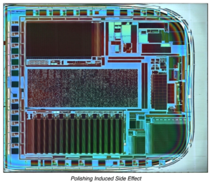
Read MCU PIC16C715 Software
Read MCU PIC16C715 Software from its flash memory, the software in the format of binary or heximal will be same as original Microcontroller PIC16C715 for the same functionality after copy content to microcontroller;
Read MCU PIC16C715 Software from its flash memory, the software in the format of binary or heximal will be same as original Microcontroller PIC16C715 for the same functionality after copy content to microcontroller
PORTB is an 8-bit wide bi-directional port. The corresponding data direction register is TRISB. Setting a bit in the TRISB register puts the corresponding output driver in a hi-impedance input mode. Clearing a bit in the TRISB register puts the contents of the output latch on the selected pin(s).
Each of the PORTB pins has a weak internal pull-up. A single control bit can turn on all the pull-ups. This is performed by clearing bit RBPU (OPTION<7>). The weak pull-up is automatically turned off when the port pin is configured as an output. The pull-ups are disabled on a Power-on Reset if extract pic16f74a MCU binary.
Four of PORTB’s pins, RB7:RB4, have an interrupt on change feature. Only pins configured as inputs can cause this interrupt to occur (i.e. any RB7:RB4 pin configured as an output is excluded from the interrupt on change comparison). The input pins (of RB7:RB4) are compared with the old value latched on the last read of PORTB. The “mismatch” outputs of RB7:RB4 are OR’ed together to generate the RB Port Change Interrupt with flag bit RBIF (INTCON<0>).
Any instruction which writes, operates internally as a read followed by a write operation. The BCF and BSF instructions, for example, read the register into the CPU, execute the bit operation and write the result back to the register. Caution must be used when these instructions are applied to a port with both inputs and outputs defined. For example, a BSF operation on bit5 of PORTB will cause all eight bits of PORTB to be read into the CPU. Then the BSF operation takes place on bit5 and PORTB is written to the output latches. If another bit of PORTB is used as a bi-directional I/O pin (e.g., bit0) and it is defined as an input at this time, the input signal present on the pin itself would be read into the CPU and rewritten to the data latch of this particular pin, overwriting the previous content. As long as the pin stays in the input mode, no problem occurs for extract microcontroller pic16c710 code. However, if bit0 is switched to an output, the content of the data latch may now be unknown.
The actual write to an I/O port happens at the end of an instruction cycle, whereas for reading, the data must be valid at the beginning of the instruction cycle (Figure 5-6). Therefore, care must be exercised if a write followed by a read operation is carried out on the same I/O port. The sequence of instructions should be such to allow the pin voltage to stabilize (load dependent) before the next instruction which causes that file to be read into the CPU is executed. Otherwise, the previous state of that pin may be read into the CPU rather than the new state. When in doubt, it is better to separate these instructions with a NOP or another instruction not accessing this I/O port.
Tags: read mcu source archive,read mcu source code,read mcu source content,read mcu source data,read mcu source eeprom,read mcu source file,read mcu source firmware,read mcu source information,read mcu source memory,read mcu source program