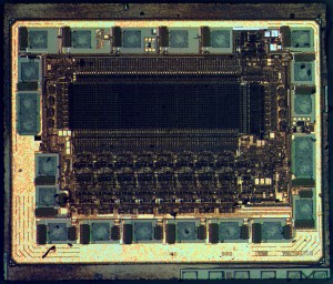
Read IC PIC MCU PIC16F887

Read IC PIC MCU PIC16F887
We can read IC PIC MCU PIC16F887, please view the chip features below for your reference:
Module: Analog-To-Digital Converter (ADC) Module
Selecting the VP6 reference as the analog input source (CHS<3:0> = 1111) for the ADC conversion after sampling another analog channel with input voltages approximately greater than 3.6V can temporarily disturb the HFINTOSC oscillator.
4. Module: MSSP (SPI Master Mode)
With MSSP in SPI Master mode, FOSC/64 or Timer2/2 clock rate and CKE = 0, a write collision may occur if SSPBUF is loaded immediately after the transfer is complete. A delay may be required after the MSSP Interrupt Flag bit, SSPIF, is set or the Buffer Full bit, BF, is set and before writing SSPBUF. If the delay is insufficiently short, a write
This only occurs when selecting the VP6 reference ADC channel using the CHS<3:0> bits in the ADCON0 collision may occur as indicated by the WCOL bit being set.
Work around
register and NOT during the start of an actual ADC conversion using the GO/DONE bit in the ADCON0 register.
Work around
Select an ADC channel with input voltages lower than 3.6V prior to selecting the VP6 reference voltage input. Any analog channel can be used, even if that channel is configured as a digital I/O (configured as an output) that is driving the output pin low when Unlock Microprocessor PIC16F873 Secured Heximal. An alternative is to configure the CVREF module to output a voltage less than 3.6V and then selecting that analog channel CHS<3:0> = 1110 as the analog input source.
Add a software delay of one SCK period after detecting the completed transfer and prior to updating the SSPBUF contents. Verify the WCOL bit is clear after writing SSPBUF. If the WCOL is set, clear the bit in software and rewrite the SSPBUF register.
Date Codes that pertain to this issue:
All engineering and production devices.
Affected Silicon Revisions
PIC16F882

