-
Product Categories
Live Support Chat


Read Chip PIC16C770 Eeprom
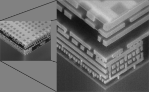
Read Chip PIC16C770 Eeprom and flash memory content after reverse engineering microcontroller and find out the location of security fuse bit, by laser cutting technique to disable it;
Read Chip PIC16C770 Eeprom and flash memory content after reverse engineering microcontroller and find out the location of security fuse bit, by laser cutting technique to disable it
This document contains device-specific information. Additional information may be found in the PICmicroTM Mid-Range Reference Manual, (DS33023), which may be obtained from your local Microchip Sales Representative or downloaded from the Microchip website. The Reference Manual should be considered a complementary document to this data sheet, and is highly recommended reading for a better understanding of the device architecture and operation of the peripheral modules.
There are two memory blocks in each of these PICmicro ® microcontrollers. Each block (Program Memory and Data Memory) has its own bus, so that concurrent access can occur. Additional information on device memory may be found in the PICmicro Mid-Range Reference Manual, (DS33023) when break MCU PIC16F630 firmware.
The PIC16C770 devices have a 13-bit program counter capable of addressing an 8K x 14 program memory space. The PIC16C717 and the PIC16C770 have 2K x 14 words of program memory.
The PIC16C771 has 4K x 14 words of program memory. Accessing a location above the physically implemented address will cause a wraparound.
The reset vector is at 0000h and the interrupt vector is at 0004h before attack mcu pic16f636 bin.
Each bank extends up to 7Fh (128 bytes). The lower locations of each bank are reserved for the Special Function Registers. Above the Special Function Registers are General Purpose Registers, implemented as static RAM. All implemented banks contain special function registers. Some frequently used special function registers from one bank are mirrored in another bank for code reduction and quicker access.
The Special Function Registers are registers used by the CPU and Peripheral Modules for controlling the desired operation of the device. These registers are implemented as static RAM for microcontroller pic16f737 flash unlocking.
The special function registers can be classified into two sets; core (CPU) and peripheral. Those registers associated with the core functions are described in detail in this section. Those related to the operation of the peripheral features are described in detail in that peripheral feature section.
Tags: read chip locked archive,read chip locked code,read chip locked content,read chip locked data,read chip locked eeprom,read chip locked file,read chip locked firmware,read chip locked information,read chip locked memory,read chip locked program
