-
Product Categories
Live Support Chat


Pull Renesas Microcontroller R5F72115D160FPV
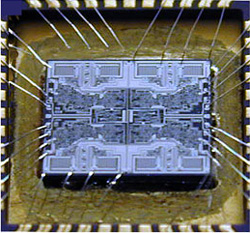
We can Unlock Microcontroller R5F72115D160FPV 32-Bit RISC Microcomputer embedded information out the encrypted system, please view the IC chip features for your reference:
Items
Specification
Compatible with SH-1 and SH-2 at object code level
32-bit internal data bus
Support of an abundant register-set
⎯ Sixteen 32-bit general registers
⎯ Four 32-bit control registers
⎯ Four 32-bit system registers
⎯ Register bank for high-speed response to interrupts
RISC-type instruction set (upward compatible with SH series)
⎯ Instruction length: 16-bit fixed-length basic instructions for improved code efficiency and 32-bit instructions for high performance and usability
⎯ Load/store architecture
⎯ Delayed branch instructions
⎯ Instruction set based on C language
Superscalar architecture to execute two instructions at one time
Instruction execution time: Up to two instructions/cycle
Address space: 4 Gbytes
Internal multiplier
Five-stage pipeline
Operating modes
Operating modes
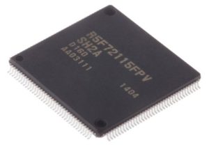
Pull Renesas Microcontroller R5F72115D160FPV
Single-chip mode
Processing states
Program execution state
Exception handling state
Bus mastership release state
Power-down modes
Sleep mode
ROM cache
Instruction/data separation system
Instruction prefetch cache: Full/set associative
Instruction prefetch miss cache: Full/set associative
Data cache: Full/set associative
Line size: 16 bytes
Hardware prefetch function (continuous/branch prefetch)
Interrupt controller
Nine external interrupt pins (NMI and IRQ7 to IRQ0) (INTC)
On-chip peripheral interrupts: Priority level set for each module 16 priority levels available
Register bank enabling fast register saving and restoring in interrupt processing
Bus state controller
Address space divided into eight areas (0 to 7), each a maximum of 64 (BSC) Mbytes
External bus: 8 or 16 bits
The following features settable for each area independently
⎯ Supports both big endian and little endian for data access
⎯ Bus size (8 or 16 bits): Available sizes depend on the area.
⎯ Number of access wait cycles (different wait cycles can be specified for read and write access cycles in some areas)
⎯ Idle wait cycle insertion (between same area access cycles or different area access cycles)
⎯ Specifying the memory to be connected to each area enables direct connection to SRAM, SRAM with byte selection, SDRAM, and burst ROM (clocked synchronous or asynchronous). The address/data multiplexed I/O (MPX) interface is also available.
⎯ Outputs a chip select signal (CS0 to CS7) according to the target area (CS assert or negate timing can be selected by software) SDRAM refresh
Auto refresh or self refresh mode selectable SDRAM burst access