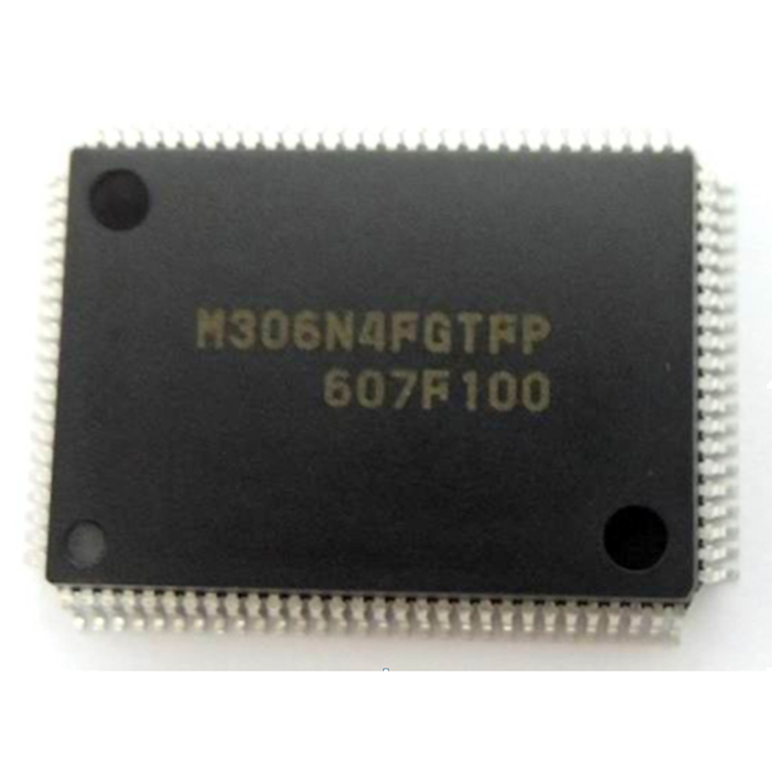
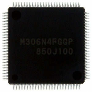
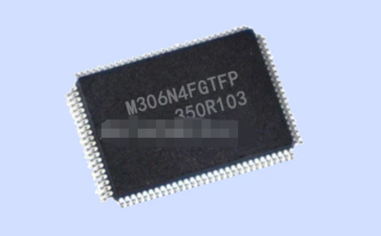
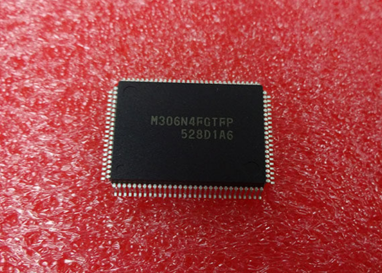
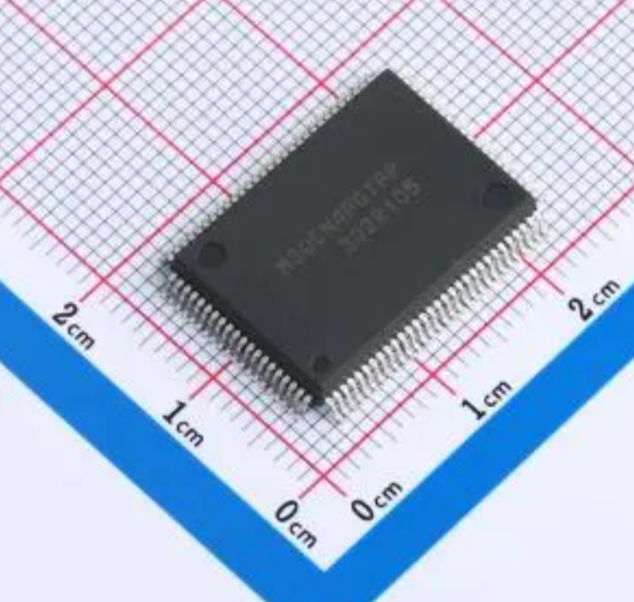
Hack MCU IC Renesas MCU M306N4FCTFP
Hack MCU IC Renesas MCU M306N4FCTFP
Hack MCU IC Renesas MCU M306N4FCTFP is a topic that frequently arises in the maintenance and long-term support of embedded systems built on classic Renesas and Hitachi microcontroller platforms. The Renesas M306N4FCTFP is a widely deployed microcontroller chip from the M16C family, valued for its stable architecture, integrated peripherals, and reliable flash and EEPROM memory organization. It has been extensively applied in industrial automation controllers, automotive subsystems, power management devices, communication equipment, metering products, and specialized consumer electronics where long service life is expected. We can Hack MCU IC Renesas MCU M306N4FCTFP, please view the chip features for your reference:
1. Overview
The M16C/6N Group (M16C/6N4) of MCUs are built using the high-performance silicon gate CMOS process using the M16C/60 Series CPU core and are packaged in 100-pin plastic molded QFP and LQFP.
These MCUs operate using sophisticated instructions featuring a high level of instruction efficiency. With 1 Mbyte of address space, they are capable of executing instructions at high speed. Being equipped with two CAN (Controller Area Network) modules in the M16C/6N Group (M16C/6N4), the MCU is suited to drive automotive and industrial control systems.
The CAN modules comply with the 2.0B specification. In addition, this MCU contains a multiplier and DMAC which combined with fast instruction processing capability, makes it suitable for control of various OA, communication, and industrial equipment which requires high-speed arithmetic/ logic operations.
1.1 Applications
· Automotive, industrial control systems and other automobile, other (T/V-ver. product)
· Car audio and industrial control systems, other (Normal-ver. product)
1.2 Performance Overview
Table 1.1 lists the Functions and Specifications for M16C/6N Group (M16C/6N4).
Table 1.1 Functions and Specifications for M16C/6N Group (M16C/6N4)
|
Item | |||
| CPU | |||
|
instructions | |||
| Minimum instruction | |||
| Operating mode | |||
| Address space | |||
| Memory capacity | |||
|
Peripheral Function |
Ports | ||
| Multifunction timers | |||
| Serial interfaces | |||
| A/D converter | |||
| D/A converter | |||
| DMAC | |||
| CRC calculation circuit | |||
| CAN module | |||
| Watchdog timer | |||
| Interrupts | |||
| Clock generation circuits | |||
| Oscillation-stopped detector | |||
|
Electrical Characteristics |
Supply voltage | ||
| Consumption |
Mask ROM | ||
| Flash memory | |||
| Mask ROM | |||
| Flash Memory | |||
| Programming and erasure endurance | |||
|
I/O Characteristics |
I/O withstand voltage | ||
| Output current | |||
|
Operating Ambient Temperature | |||
|
Device Configuration | |||
|
Package | |||
|
Specification | |
|
Normal-ver. |
T/V-ver. |
|
91 instructions | |
|
41.7 ns (f(BCLK) = 24 MHz, 1/1 prescaler, without software wait) |
1/1 prescaler, without software wait) |
|
Single-chip, memory expansion, and microprocessor modes | |
|
1 Mbyte | |
|
Refer to Table 1.2 Product Information | |
|
Input/Output: 87 pins, Input: 1 pin | |
|
Timer A: 16 bits ✕ 5 channels Timer B: 16 bits ✕ 6 channels Three-phase motor control circuit | |
|
3 channels 2 (1) (2) Clock synchronous, UART, I C-bus , IEBus 1 channel Clock synchronous | |
|
10-bit A/D converter: 1 circuit, 26 channels | |
|
8 bits ✕ 2 channels | |
|
2 channels | |
|
CRC-CCITT | |
|
2 channels with 2.0B specification | |
|
15 bits ✕ 1 channel (with prescaler) | |
|
Internal: 31 sources, External: 9 sources Software: 4 sources, Priority levels: 7 levels | |
|
4 circuits · Main clock oscillation circuit (*) · Sub clock oscillation circuit (*) · On-chip oscillator · PLL frequency synthesizer (*) Equipped with on-chip feedback resistor | |
|
Main clock oscillation stop and re-oscillation detection function | |
|
VCC = 3.0 to 5.5 V (f(BCLK) = 24 MHz, 1/1 prescaler, without software wait) |
VCC = 4.2 to 5.5 V (f(BCLK) = 20 MHz, 1/1 prescaler, without software wait) |
|
20 mA (f(BCLK) = 24 MHz, PLL operation, no division) |
18 mA (f(BCLK) = 20 MHz, PLL operation, no division) |
|
22 mA (f(BCLK) = 24 MHz, PLL operation, no division) |
20 mA (f(BCLK) = 20 MHz, PLL operation, no division) |
|
3 µA (f(BCLK) = 32 kHz, Wait mode, Oscillation capacity Low) | |
|
0.8 µA (Stop mode, Topr = 25°C) | |
|
3.0 ± 0.3 V or 5.0 ± 0.5 V |
5.0 ± 0.5 V |
|
100 times | |
|
5.0 V | |
|
5 mA | |
|
-40 to 85°C |
T version: -40 to 85°C V version: -40 to 125°C (option) |
|
CMOS high-performance silicon gate | |
|
100-pin molded-plastic QFP, LQFP | |
NOTES:
1. I2C-bus is a trademark of Koninklijke Philips Electronics N.V.
2. IEBus is a trademark of NEC Electronics Corporation.
option: All options are on request basis.
In many real-world cases, the embedded firmware exists only as a compiled binary or heximal file stored internally, while the original source code, development archive, or programming documentation has been lost, making it difficult to maintain, upgrade, or replicate the system when hardware issues or supply constraints occur. The challenge with the M306N4FCTFP MCU is that it is typically delivered in a secured, protected, and often encrypted or locked configuration, with readout protection enabled to prevent unauthorized access to the internal program and configuration data. As a result, standard debugging tools cannot perform a direct readout, nor can engineers simply copy or dump the contents of the on-chip flash without specialized expertise.
Attempting to crack, decrypt, or force access without proper technical control can permanently damage the chip, erase the internal memory, or corrupt timing-critical logic, which makes recovery significantly more complex. From a technical standpoint, the difficulty lies in preserving data integrity while safely bypassing protection mechanisms so the embedded binary file can be accurately retrieved, replicated, or restored for analysis and reuse.
The purpose of performing this type of controlled unlock operation is not curiosity, but continuity: enabling manufacturers to recover legacy control logic, duplicate proven designs, validate field-deployed systems, or migrate functionality to new microprocessor platforms without redesigning from scratch. Our service capability focuses on reliable, non-destructive solutions tailored to Renesas MCUs, allowing customers to safely recover and restore embedded firmware while minimizing risk to the original device.
By handling each project with careful assessment of protection status, silicon condition, and application context, we ensure that valuable embedded program assets stored inside a locked M306N4FCTFP MCU can be extracted and preserved. For industries that depend on stable operation, regulatory compliance, or uninterrupted production, the ability to securely unlock and extract firmware from a protected Renesas microcontroller provides a practical and effective path to extending product life cycles and safeguarding critical embedded technology.