-
Product Categories
Live Support Chat


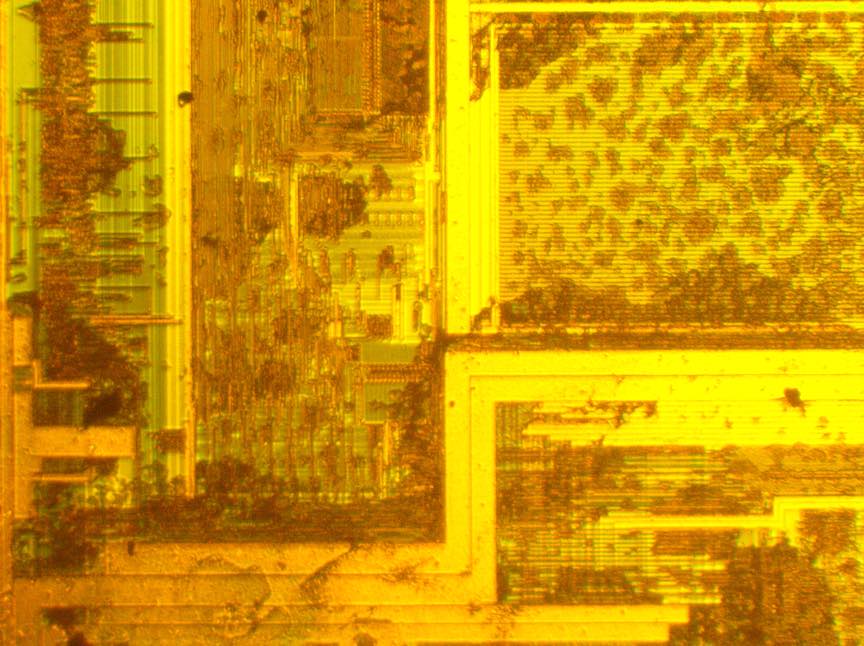
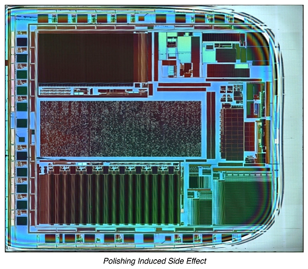
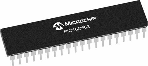
Extract MCU PIC16C662 Heximal
Extract MCU PIC16C662 Heximal from embedded flash memory can help engineer to recover the lost heximal file from microcontroller pic16c662 and copy firmware to new MCU;
The clock input (from OSC1) is internally divided by four to generate four non-overlapping quadrature clocks namely Q1, Q2, Q3, and Q4. Internally, the program counter (PC) is incremented every Q1, the instruction is fetched from the program memory and latched into the instruction register in Q4. The instruction is decoded and executed during the following Q1 through Q4. The clocks and instruction execution flow is shown in Figure 3-3 if unlocking microchip pic12f510 MCU.
An “Instruction Cycle” consists of four Q cycles (Q1, Q2, Q3, and Q4). The instruction fetch and execute are pipelined such that fetch takes one instruction cycle while decode and execute takes another instruction cycle. However, due to the pipelining, each instruction effectively executes in one cycle.
If an instruction causes the program counter to change (e.g., GOTO) then two cycles are required to complete the instruction (Example 3-1). A fetch cycle begins with the program counter (PC) incrementing in Q1.
In the execution cycle, the fetched instruction is latched into the “Instruction Register (IR)” in cycle Q1. This instruction is then decoded and executed during the Q2, Q3, and Q4 cycles. Data memory is read during Q2 (operand read) and written during Q4 (destination write) if Extract microchip pic16f72 MCU code.
The PIC16C64X & PIC16C66X have a 13-bit program counter capable of addressing an 8K x 14 program memory space. For the PIC16C641 and PIC16C661 only the first 2K x 14 (0000h – 07FFh) is physically implemented. For the PIC16C642 and PIC16C662 only the first 4K x 14 (0000h – 0FFh) is physically implemented before Extract MCU.
Accessing a location above the 2K or 4K boundary will cause a wrap-around. The reset vector is at 0000h and the interrupt vector is at 0004h (Figure 4- 1 and Figure 4-2). See Section 4.4 for Program Memory paging. The data memory (Figure 4-4) is partitioned into two banks which contain the general purpose registers and the special function registers when Extract MCU.
Bank 0 is selected when bit RP0 (STATUS<5>) is cleared. Bank 1 is selected when the RP0 bit is set. The Special Function Registers are located in the first 32 locations of each Bank before Extract MCU.
Register locations A0h-EFh (Bank 1) are general purpose registers implemented as static RAM. Some special function registers are mapped in Bank 1. The register file is organized as 176 x 8 for the PIC16C642/662, and 128 x8 for the PIC16C641/661. Each is accessed either directly, or indirectly through the File Select Register FSR (Section 4.5).