-
Product Categories
Live Support Chat


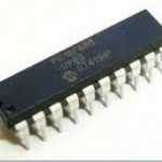
Extract Chip PIC18F8620 Code
Extract Chip PIC18F8620 Code in the format of heximal or binary from the locked memory include flash and eeprom, then copy the data and program into other blank Microcontroller PIC18F8620;
Extract Chip PIC18F8620 Code in the format of heximal or binary
Note 1:
Alternate assignment for CCP2 when CCP2MX is not selected (all operating modes except Microcontroller).
Default assignment when CCP2MX is set.
External memory interface functions are only available on PIC18F8X20 devices.
CCP2 is multiplexed with this pin by default when configured in Microcontroller mode. Otherwise, it is multiplexed with either RB3 or RC1.
PORTH and PORTJ are only available on PIC18F8X20 (80-pin) devices.
AVDD must be connected to a positive supply and AVSS must be connected to a ground reference for proper operation of the part in user or ICSP modes. See parameter D001A for details.
Note 1:
Alternate assignment for CCP2 when CCP2MX is not selected (all operating modes except Microcontroller).
Default assignment when CCP2MX is set.
External memory interface functions are only available on PIC18F8X20 devices.
CCP2 is multiplexed with this pin by default when configured in Microcontroller mode. Otherwise, it is multiplexed with either RB3 or RC1.
PORTH and PORTJ are only available on PIC18F8X20 (80-pin) devices.
AVDD must be connected to a positive supply and AVSS must be connected to a ground reference for proper operation of the part in user or ICSP modes which has been applied for the upcoming MCU program recovering. See parameter D001A for details.
An external clock source may also be connected to the OSC1 pin in the HS, XT and LP modes, as shown in
For timing insensitive applications, the “RC” and “RCIO” device options offer additional cost savings.
The RC oscillator frequency is a function of the supply voltage, the resistor (REXT) and capacitor (CEXT) values and the operating temperature. In addition to this, the oscillator frequency will vary from unit to unit, due to normal process parameter variation.
Furthermore, the difference in lead frame capacitance between package types will also affect the oscillation frequency, especially for low CEXT values. The user also needs to take into account variation due to tolerance of external R and C components used. Figure 2-3 shows how the R/C combination is connected.
The RCIO Oscillator mode functions like the RC mode, except that the OSC2 pin becomes an additional general purpose I/O pin. The I/O pin becomes bit 6 of PORTA (RA6).
Tags: extract chip dump archive,extract chip dump code,extract chip dump content,extract chip dump data,extract chip dump eeprom,extract chip dump file,extract chip dump firmware,extract chip dump information,extract chip dump memory,extract chip dump program