-
Product Categories
Live Support Chat


Extract Chip PIC16C77 Code
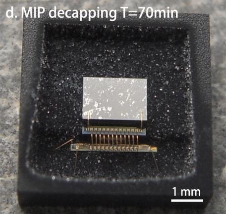
Extract Chip PIC16C77 Code from microcontroller, the embedded flash content will be copied from mcu pic16c77 to new MCU, as a result of that the original microcontroller pic16c77 functionality will be recovered;
There are actually two 8-bit latches, one for data-out (from the PIC16/17) and one for data input. The user writes 8-bit data to PORTD data latch and reads data
Chip Select from the port pin latch (note that they have the same address). In this mode, the TRISD register is ignored, since the microprocessor is controlling the direction of A write to the PSP occurs when both the CS and WR lines are first detected low. When either the CS or WR lines become high (level triggered) if Extract Chip, then the Input Buffer Full status flag bit IBF (TRISE<7>) is set on the Q4 clock cycle, following the next Q2 cycle, to signal the write is complete (Figure 5-12). The interrupt flag bit PSPIF (PIR1<7>) is also set on the same Q4 clock cycle. IBF can only be cleared by reading the PORTD input latch. The input Buffer Overflow status flag bit IBOV (TRISE<5>) is set if a second write to the Parallel Slave Port is attempted when the previous byte has not been read out of the buffer. A read from the PSP occurs when both the CS and RD lines are first detected low. The Output Buffer Full status flag bit OBF (TRISE<6>) is cleared immediately (Figure 5-13) indicating that the PORTD latch is waiting to be read by the external bus before Extract Chip. When either the CS or RD pin becomes high (level triggered), the interrupt flag bit PSPIF is set on the Q4 clock cycle, following the next Q2 cycle, indicating that the read is complete. OBF remains low until data is written to PORTD by the user firmware after Extract Chip.
When not in Parallel Slave Port mode, the IBF and OBF bits are held clear. However, if flag bit IBOV was previously set, it must be cleared in firmware. An interrupt is generated and latched into flag bit PSPIF when a read or write operation is completed. PSPIF must be cleared by the user in firmware and the interrupt can be disabled by clearing the interrupt enable bit PSPIE (PIE1<7>).
The Timer0 module is a simple 8-bit overflow counter.
The clock source can be either the internal system clock (Fosc/4) or an external clock. When the clock CCP Overview source is an external clock, the Timer0 module can be selected to increment on either the rising or falling edge.
The Timer0 module also has a programmable prescaler option. This prescaler can be assigned to either the Timer0 module or the Watchdog Timer. Bit PSA (OPTION<3>) assigns the prescaler, and bits PS2:PS0 (OPTION<2:0>) determine the prescaler value. Timer0 can increment at the following rates: 1:1 (when pres-caler assigned to Watchdog timer), 1:2, 1:4, 1:8, 1:16, 1:32, 1:64, 1:128, and 1:256 (Timer0 only) if read microchip pic mcu 12f508.
Synchronization of the external clock occurs after the prescaler. When the prescaler is used, the external clock frequency may be higher then the device’s frequency. The maximum frequency is 50 MHz, given the high and low time requirements of the clock Timer1 is a 16-bit timer/counter. The clock source can be either the internal system clock (Fosc/4), an external clock, or an external crystal.
Timer1 can operate as either a timer or a counter. When operating as a counter (external clock source), the counter can either operate synchronized to the device or asynchronously to the device. Asynchronous operation allows Timer1 to operate during sleep, which is useful for applications that require a real-time clock as well as the power savings of SLEEP mode before decode pic mcu 16f505.
Timer1 also has a prescaler option which allows Timer1 to increment at the following rates: 1:1, 1:2, 1:4, and 1:8. Timer1 can be used in conjunction with the Capture/Compare/PWM module. When used with a CCP module, Timer1 is the time-base for 16-bit Capture or the 16-bit Compare and must be synchronized to the device.
The CCP module(s) can operate in one of these three modes: 16-bit capture, 16-bit compare, or up to 10-bit Pulse Width Modulation (PWM). Capture mode captures the 16-bit value of TMR1 into the CCPRxH:CCPRxL register pair. The capture event can be programmed for either the falling edge, rising edge, fourth rising edge, or the sixteenth rising edge of the CCPx pin.
Compare mode compares the TMR1H:TMR1L register pair to the CCPRxH:CCPRxL register pair. When a match occurs an interrupt can be generated, and the output pin CCPx can be forced to given state (High or Low), TMR1 can be reset (CCP1), or TMR1 reset and start A/D conversion (CCP2). This depends on the control bits CCPxM3:CCPxM0. PWM mode compares the TMR2 register to a 10-bit duty cycle register (CCPRxH:CCPRxL<5:4>) before Extract Chip.
Tags: çatlamak chip,çatlamak entegre devre,çatlamak ic,çatlamak mcu,çatlamak mikrodenetleyici,çatlamak yonga,kırmak chip,kırmak entegre devre,kırmak ic,kırmak mcu,kırmak mikrodenetleyici,kırmak yonga