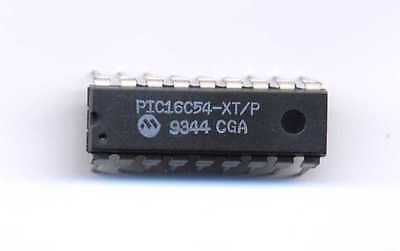
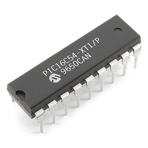
Duplicate PIC16C54 Microcontroller Memory Program
Duplicate PIC16C54 locked microcontroller memory program starts from break secured microprocessor PIC16C54 fuse bit and extract protective Microchip MCU PIC16C54 embedded firmware in the format of binary file or heximal data;
The PIC16C54 device contains an 8-bit ALU and working register. The ALU is a general purpose arithmetic unit. It performs arithmetic and Boolean functions between data in the working register and any register file to Duplicate PIC16C54 Microcontroller Memory Program.
The ALU is 8-bits wide and capable of addition, subtraction, shift and logical operations when Crack Microcontroller dsPIC30F3014 Binary. Unless otherwise mentioned, arithmetic operations are two’s complement in nature. In two-operand instructions, typically one operand is the W (working) register.
The other operand is either a file register or an immediate constant. In single operand instructions, the operand is either the W register or a file register. The W register is an 8-bit working register used for ALU operations after Crack MCU dsPIC30F6010A Eeprom. It is not an addressable register.
Depending on the instruction executed, the ALU may affect the values of the Carry (C), Digit Carry (DC), and Zero (Z) bits in the STATUS register. The C and DC bits operate as a borrow and digit borrow out bit, respectively, in subtraction. See the SUBWF and ADDWF instructions for examples.
A simplified block diagram is shown in below Figure
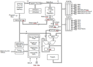
The clock input (OSC1/CLKIN pin) is internally divided by four to generate four non-overlapping quadrature clocks namely Q1, Q2, Q3 and Q4. Internally, the program counter is incremented every Q1 from Replicate S3F84U8 Microcontroller Flash Heximal, and the instruction is fetched from program memory and latched into instruction register in Q4 to Duplicate PIC16C54 Microcontroller Memory Program. It is decoded and executed during the following Q1 through Q4.
An Instruction Cycle consists of four Q cycles (Q1, Q2, Q3 and Q4). The instruction fetch and execute are pipelined such that fetch takes one instruction cycle while decode and execute takes another instruction cycle. However, due to the pipelining, each instruction effectively executes in one cycle in order to Replicate MC68HC11A8 MCU Memory Program. If an instruction causes the program counter to change (e.g., GOTO) then two cycles are required to complete the instruction (Example 3-1).
A fetch cycle begins with the program counter (PC) incrementing in Q1. In the execution cycle, the fetched instruction is latched into the Instruction Register (IR) in cycle Q1. This instruction is then decoded and executed during the Q2, Q3, and Q4 cycles to facilitate the process of Reverse Microcontroller Data. Data memory is read during Q2 (operand read) and written during Q4 (destination write).