-
Product Categories
Live Support Chat


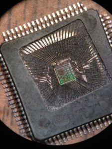
Decrypt Chip HOLTEK HT48R50A-1 I/O Type 8-Bit MCU
Decrypt Chip HOLTEK HT48R50A-1 I/O Type 8-Bit MCU
We can Decrypt Chip HOLTEK HT48R50A-1 I/O Type 8-Bit MCU, please view the IC Chip features for your reference:
Features
- · Operating voltage:
fSYS=4MHz: 2.2V~5.5V
fSYS=8MHz: 3.3V~5.5V
- · Low voltage reset function
- · 35 bidirectional I/O lines (max.)
- · 1 interrupt input shared with an I/O line
- · 8-bit programmable timer/event counter with overflow interrupt and 8-stage prescaler
- · 16-bit programmable timer/event counter and over-flow interrupts
- · On-chip RC oscillator, external crystal and RC oscillator
- · 32768Hz crystal oscillator for timing purposes only
- · Watchdog Timer
General Description
The HT48R50A-1/HT48C50-1 are 8-bit high performance, RISC architecture microcontroller devices specifically designed for multiple I/O control product applications. The mask version HT48C50-1 is fully pin and functionally compatible with the OTP version HT48R50A-1 device.
- · 4096´15 program memory ROM
- · 160´8 data memory RAM
- · Buzzer driving pair and PFD supported
- · HALT function and wake-up feature reduce power consumption
- · 6-level subroutine nesting
- · Up to 0.5ms instruction cycle with 8MHz system clock at VDD=5V
- · Bit manipulation instruction
- · 15-bit table read instruction
- · 63 powerful instructions
- · All instructions in one or two machine cycles
- · 28-pin SKDIP/SOP, 48-pin SSOP package
The advantages of low power consumption, I/O flexibility, timer functions, oscillator options, HALT and wake-up functions, watchdog timer, buzzer driver, as well as low cost, enhance the versatility of these devices to suit a wide range of application possibilities such as industrial control, consumer products, subsystem controllers, etc.
Functional Description
Execution Flow
The system clock for the microcontroller is derived from either a crystal or an RC oscillator. The system clock is internally divided into four non-overlapping clocks. One instruction cycle consists of four system clock cycles. Instruction fetching and execution are pipelined in such a way that a fetch takes an instruction cycle while decoding and execution takes the next instruction cycle. However, the pipelining scheme causes each instruction to effectively execute in a cycle. If an instruction changes the program counter, two cycles are required to complete the instruction.
Program Counter – PC
The program counter (PC) controls the sequence in which the instructions stored in the program ROM are executed and its contents specify a full range of program memory. After accessing a program memory word to fetch an instruction code, the contents of the program counter are incremented by one.
The program counter then points to the memory word containing the next instruction code. When executing a jump instruction, conditional skip execution, loading PCL register, subroutine call, initial reset, internal interrupt, external interrupt or return from subroutine, the PC manipulates the program transfer by loading the address corresponding to each instruction.
The conditional skip is activated by instructions. Once the condition is met, the next instruction, fetched during the current instruction execution, is discarded and a dummy cycle replaces it to get the proper instruction. Otherwise proceed with the next instruction. The lower byte of the program counter (PCL) is a readable and writeable register (06H). Moving data into the PCL performs a short jump. The destination will be within 256 locations.
When a control transfer takes place, an additional dummy cycle is required.
Program Memory – ROM
The program memory is used to store the program instructions which are to be executed. It also contains data, table, and interrupt entries, and is organized into 4096´15 bits, addressed by the program counter and table pointer.