-
Product Categories
Live Support Chat


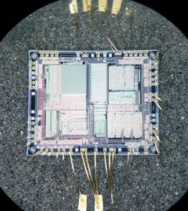
Decipher Microprocessor IC Motorola MC9S12B128 16-Bit Microcontroller
Designed for automotive multiplexing applications, members of the MC9S12B-Family of 16 bit Flash-based microcontrollers are fully pin compatible and enable users to choose between different memory and peripheral options for scalable designs to facilitate process of Decipher Microprocessor IC Motorola MC9S12B128 16-Bit Microcontroller.
All MC9S12B-Family members are composed of standard on-chip peripherals including a 16-bit central processing unit (CPU12), up to 256K bytes of Flash EEPROM, 8K bytes of RAM, 2K bytes of EEPROM, two asynchronous serial communications interfaces (SCI), serial peripheral interface (SPI), an input capture/output compare timer (TIM), 16-channel, 10-bit analog-to-digital converter (ADC), an 8-channel pulse-width modulator (PWM), one CAN 2.0 A, B software compatible module (MSCAN12) and an Inter-IC Bus.
System resource mapping, clock generation, interrupt control and bus interfacing are managed by the lite integration module (LIM). The MC9S12B-Family has full 16-bit data paths throughout, however, the external bus can operate in an 8-bit narrow mode so single 8-bit wide memory can be interfaced for lower cost systems.
The inclusion of a PLL circuit allows power consumption and performance to be adjusted to suit operational requirements. In addition to the I/O ports available in each module, up to 22 I/O ports are available with Wake-Up capability from STOP or WAIT mode.
Not all features listed here are available in all configurations.
Decipher Microprocessor IC Motorola MC9S12B128 16-Bit Microcontroller
Additional information about D and B family inter-operability is given in:
EB386 “HCS12 D-Family Compatibility Considerations” and
EB388 “Using the HCS12 D_Family as a development platform for the HCS12 B family”
· 16-bit CPU12
— Upward compatible with M68HC11 instruction set
— Interrupt stacking and programmer’s model identical to M68HC11
— 20-bit ALU
— Instruction queue
— Enhanced indexed addressing
· Multiplexed bus
— Single chip or expanded
— 16 address/16 data wide or 16 address/8 data narrow modes
— External address space 1MByte for Data and Program space (112 pin package only)
· Wake-up interrupt inputs depending on the package option
— 8-bit port H
— 4-bit port J
— 8-bit port P shared with PWM
· Memory options
— 64K, 128K, 256K Byte Flash EEPROM
— 1K, 2K Byte EEPROM
— 2K, 4K and 8K Byte RAM
Analog-to-Digital Converter
— 16-channels for 112 Pin Package, 8 channels for 80 Pin package options, 10-bit resolution
— External conversion trigger capability to Pull Freescale Microcontroller MC9S12XS128MAL Program
· 1M bit per second, CAN 2.0 A, B software compatible module
— Five receive and three transmit buffers
— Flexible identifier filter programmable as 2 x 32 bit, 4 x 16 bit or 8 x 8 bit
— Four separate interrupt channels for Rx, Tx, error and wake-up
— Low-pass filter wake-up function
— Loop-back for self test operation
· Input Capture/Output Compare Timer (TIM)
— 16-bit Counter with 7-bit Prescaler
— 8 programmable input capture or output compare channels
— Simple PWM Mode
— Modulo Reset of Timer Counter
— 16-bit Pulse Accumulator
— External Event Counting
— Gated Time Accumulation
· 8 PWM channels with programmable period and duty cycle (7 channels on 80 Pin Packages)
— 8-bit 8-channel or 16-bit 4-channel
— Separate control for each pulse width and duty cycle
— Center- or left-aligned outputs
— Programmable clock select logic with a wide range of frequencies
· Serial interfaces
— Two asynchronous serial communications interfaces (SCI)
— synchronous serial peripheral interface (SPI)
· Inter-IC Bus (IIC)
— Compatible with I2C Bus standard
— Multi-master operation
— Software programmable for one of 256 different serial clock frequencies
· SIM (System Integration Module)
— CRG (windowed COP watchdog, real time interrupt, clock monitor, clock generation and reset)
— MEBI (multiplexed external bus interface)
— MMC (memory map and interface)
— INT (interrupt control)
— BKP (breakpoints)
— BDM (background debug mode)
· Clock generation
— Phase-locked loop clock frequency multiplier
— Limp home mode in absence of external clock in order to break IC program
— Clock Monitor
— Low power 0.5 to 16 MHz crystal oscillator reference clock
· Operation frequency
— 32MHz equivalent to 16MHz Bus Speed for single chip
— 32MHz equivalent to 16MHz Bus Speed in expanded bus modes
— Option: 50MHz equivalent to 25Mhz Bus Speed
· Internal 5V to 2.5V Regulator
· 112-Pin or 80-Pin LQFP package
— I/O lines with 5V input and drive capability
— 5VA/D converter inputs
— Dual supply – 5V for I/O and A/D, 2.5V logic
Tags: decipher microprocessor ic binary data,decipher microprocessor ic dump information,decipher microprocessor ic embed firmware,decipher microprocessor ic encrypt program,decipher microprocessor ic flash content,decipher microprocessor ic heximal file,decipher microprocessor ic protect eprom,decipher microprocessor ic software memory,decipher microprocessor ic source code