-
Product Categories
Live Support Chat


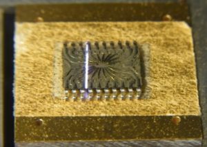
Crack Protected Microcontroller PIC18F2510 Program
Crack Protected Microcontroller PIC18F2510 Program from its locked flash and eeprom memory, then read the program or data out from its memory for a matching cloning units:
The IDLEN bit determines if the device goes into Sleep mode or one of the Idle modes when the SLEEP instruction is executed. The use of the flag and control bits in the OSCCON register is discussed in more detail in Section 3.0 “Power Managed Modes”.
Crack Protected Microcontroller PIC18F2510 Program
Note 1: The Timer1 oscillator must be enabled to select the secondary clock source. The Timer1 oscillator is enabled by setting the T1OSCEN bit in the Timer1 Control register (T1CON<3>). If the Timer1 oscillator is not enabled, then any attempt to select a secondary clock source will be ignored.
2: It is recommended that the Timer1 oscillator be operating and stable before selecting the secondary clock source or a very long delay may occur while the Timer1 oscillator starts.
PIC18F2510 devices contain circuitry to prevent clock “glitches” when switching between clock sources. A short pause in the device clock occurs during the clock switch. The length of this pause is the sum of two cycles of the old clock source and three to four cycles of the new clock source. This formula assumes that the new clock source is stable.
When PRI_IDLE mode is selected, the designated primary oscillator continues to run without interruption. For all other power managed modes, the oscillator using the OSC1 pin is disabled. The OSC1 pin (and OSC2 pin, if used by the oscillator) will stop oscillating.
In secondary clock modes (SEC_RUN and SEC_IDLE), the Timer1 oscillator is operating and providing the device clock. The Timer1 oscillator may also run in all power managed modes if required to clock Timer1 or Timer3.
In internal oscillator modes (RC_RUN and RC_IDLE), the internal oscillator block provides the device clock source.
The 31 kHz INTRC output can be used directly to provide the clock and may be enabled to support various special features, regardless of the power managed mode (see Section 23.2 “Watchdog Timer (WDT)”, Section 23.3 “Two-Speed Start-up” and Section 23.4 “Fail-Safe Clock Monitor” for more information on WDT, Fail-Safe Clock Monitor and Two-Speed Start-up).
The INTOSC output at 8 MHz may be used directly to clock the device or may be divided down by the postscaler. The INTOSC output is disabled if the clock is provided directly from the INTRC output. If the Sleep mode is selected, all clock sources are stopped. Since all the transistor switching currents have been stopped, Sleep mode achieves the lowest current consumption of the device (only leakage currents).