-
Product Categories
Live Support Chat


Crack Microcontroller PIC18F8393 Program
Crack Microcontroller PIC18F8393 flash and eeprom memory, extract the program and data from the memory and replicate the content and firmware to other blank MCU PIC18F8393;
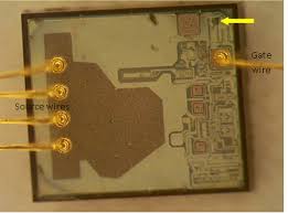
Crack Microcontroller PIC18F8393 Program
The analog reference voltage is software selectable to either the device’s positive and negative supply voltage (VDD and VSS), or the voltage level on the RA3/AN3/VREF+/SEG17 and RA2/AN2/VREF-/SEG16 pins.
The A/D Converter has a unique feature of being able to operate while the device is in Sleep mode. To operate in Sleep, the A/D conversion clock must be derived from the A/D’s internal RC oscillator.
The output of the sample and hold is the input into the converter, which generates the result via successive approximation. A device Reset forces all registers to their Reset state. This forces the A/D module to be turned off and any conversion in progress is aborted.
Each port pin associated with the A/D Converter can be configured as an analog input or a digital I/O. The ADRESH and ADRESL registers contain the result of the A/D conversion. When the A/D conversion is complete, the result is loaded into the ADRESH:ADRESL register pair, the GO/DONE bit (ADCON0<1>) is cleared and the A/D Interrupt Flag bit, ADIF, is set.
The block diagram of the A/D module is shown in Figure 2-1. The value in the ADRESH:ADRESL registers is unknown following Power-on and Brown-out Resets and is not affected by any other Reset.
After the A/D module has been configured as desired, the selected channel must be acquired before the conversion is started. The analog input channels must have their corresponding TRIS bits selected as an input. To determine acquisition time.
After this acquisition time has elapsed, the A/D conversion can be started. An acquisition time can be programmed to occur between setting the GO/DONE bit and the actual start of the conversation.
The following steps should be followed to perform an A/D conversion:
. Configure the A/D module:
· Configure analog pins, voltage reference and digital I/O (ADCON1)
· Select A/D input channel (ADCON0)
· Select A/D acquisition time (ADCON2)
· Select A/D conversion clock (ADCON2)
Turn on A/D module (ADCON0) Configure A/D interrupt (if desired):
· Clear ADIF bit
· Set ADIE bit
· Set GIE bit
Wait the required acquisition time (if required).
Start conversion:
· Set GO/DONE bit (ADCON0<1>)
For the A/D Converter to meet its specified accuracy, the charge holding capacitor (CHOLD) must be allowed to fully charge to the input channel voltage level.
The source impedance (RS) and the internal sampling switch (RSS) impedance directly affect the time required to charge the capacitor, CHOLD. The sampling switch (RSS) impedance varies over the device voltage (VDD). The source impedance affects the offset voltage at the analog input to copy microcontroller software (due to pin leakage current).
The maximum recommended impedance for analog sources is 2.5 kÙ. After the analog input channel is selected (changed), the channel must be sampled for at least the minimum acquisition time before starting a conversion.
Tags: crack microcontroller source archive,crack microcontroller source code,crack microcontroller source content,crack microcontroller source data,crack microcontroller source eeprom,crack microcontroller source file,crack microcontroller source firmware,crack microcontroller source information,crack microcontroller source memory,crack microcontroller source program
