-
Product Categories
Live Support Chat


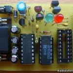
Crack Microcontroller PIC18F448 Heximal
Crack Microcontroller PIC18F448 will need to modify the circuit layout of the MCU through which the status of MCU can be changed from locked to unlocked and then the Heximal inside the MCU memory will be free to readout;
Crack Microcontroller PIC18F448 will need to modify the circuit layout of the MCU through which the status of MCU can be changed from locked to unlocked and then the Heximal inside the MCU memory will be free to readout;
The PIC18FXX8 devices contain circuitry to prevent “glitches” when switching between oscillator sources.
Essentially, the circuitry waits for eight rising edges of the clock source that the processor is switching to. This ensures that the new clock source is stable and that its pulse width will not be less than the shortest pulse width of the two clock sources.
Figure 2-7 shows a timing diagram indicating the transition from the main oscillator to the Timer1 oscillator. The Timer1 oscillator is assumed to be running all the time.
After the SCS bit is set, the processor is frozen at the next occurring Q1 cycle. After eight synchronization cycles are counted from the Timer1 oscillator, operation resumes. No additional delays are required after the synchronization cycles if Copy pic mcu flash.
There are three memory blocks in Enhanced MCU devices. These memory blocks are:
· Enhanced Flash Program Memory
· Data Memory
· EEPROM Data Memory
Data and program memory use separate busses, which allows concurrent access of these blocks. Additional detailed information on data EEPROM and Flash program memory is provided in Section 5.0 “Data EEPROM Memory” and Section 6.0 “Flash Program Memory”, respectively.
The PIC18F258/458 devices have a 21-bit program counter that is capable of addressing a 2-Mbyte program memory space. The Reset vector address is at 0000h and the interrupt vector addresses are at 0008h and 0018h after Crack pic mcu dump.
The PIC18F258 and the PIC18F458 have 32 Kbytes of internal Enhanced Flash program memory. This means that the PIC18F258 and the PIC18F458 can store up to 16K of single-word instructions. The PIC18F248 and PIC18F448 have 16 Kbytes of Enhanced Flash program memory.
This translates into 8192 single-word instructions, which can be stored in the program memory. Accessing a location between the physically implemented memory and the 2-Mbyte address willcause a read of all ‘0’s (a NOP instruction).
The return address stack allows any combination of up to 31 program calls and interrupts to occur. The PC (Program Counter) is pushed onto the stack when a PUSH, CALL or RCALL instruction is executed, or an interrupt is Acknowledged.
The PC value is pulled off the stack on a RETURN, RETLW or a RETFIE instruction. PCLATU and PCLATH are not affected by any of the RETURN instructions when reverse engineering pic mcu.
The stack operates as a 31-word by 21-bit stack memory and a 5-bit Stack Pointer register, with the Stack Pointer initialized to 00000b after all Resets. There is no RAM associated with Stack Pointer 00000b.
This is only a Reset value. During a CALL type instruction, causing a push onto the stack, the Stack Pointer is first incremented and the RAM location pointed to by the Stack Pointer is written with the contents of the PC.
During a RETURN type instruction, causing a pop from the stack, the contents of the RAM location indicated by the STKPTR are transferred to the PC and then the Stack Pointer is decremented.
The stack space is not part of either program or data space. The Stack Pointer is readable and writable and the data on the top of the stack is readable and writable through SFR registers. Status bits indicate if the stack pointer is at or beyond the 31 levels provided.
Tags: crack microcontroller heximal archive,crack microcontroller heximal code,crack microcontroller heximal content,crack microcontroller heximal data,crack microcontroller heximal eeprom,crack microcontroller heximal file,crack microcontroller heximal firmware,crack microcontroller heximal information,crack microcontroller heximal memory,crack microcontroller heximal program