-
Product Categories
Live Support Chat


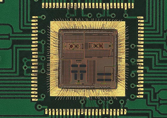
Crack Microcontroller PIC16F722 Code
Crack Microcontroller PIC16F722 and read mcu pic16f722 encrypted code from flash memory, reverse engineering pic16f722 microcontroller to locate the security fuse bit of it;
High-Performance RISC CPU:
· Only 35 Instructions to Learn:
– All single-cycle instructions except branches
· Operating Speed:
– DC – 20 MHz oscillator/clock input
– DC – 200 ns instruction cycle
· Up to 8K x 14 Words of Flash Program Memory
· Up to 368 Bytes of Data Memory (RAM)
· Interrupt Capability
· 8-Level Deep Hardware Stack if unlocking pic16f767 Microcontroller memory
· Direct, Indirect and Relative Addressing modes
· Processor Read Access to Program Memory
· Pinout Compatible to other 28/40-pin PIC16CXXX and PIC16FXXX Microcontrollers
Special Microcontroller Features:
· Precision Internal Oscillator:
– 16 MHz or 500 kHz operation
– Factory calibrated to ±1%, typical
– Software tunable
– Software selectable ÷1, ÷2, ÷4 or ÷8 divider
· 1.8V-5.5V Operation – PIC16F72X
· 1.8V-3.6V Operation – PIC16LF72X after Crack freescale mc68hc705p6a Microcontroller
· Power-on Reset (POR), Power-up Timer (PWRT) and Oscillator Start-up Timer (OST)
· Brown-out Reset (BOR):
– Selectable between two trip points
– Disable in Sleep option
· Programmable Code Protection
· In-Circuit Serial ProgrammingTM (ICSPTM) via Two Pins
· Multiplexed Master Clear with Pull-up/Input Pin
· Industrial and Extended Temperature Range
· High-Endurance Flash Cell:
– 1,000 write Flash endurance (typical)
– Flash retention: > 40 years
· Power-Saving Sleep mode
Peripheral Highlights:
· Up to 35 I/O Pins and 1 Input-only Pin:
– High-current source/sink for direct LED drive
– Interrupt-on-pin change
– Individually programmable weak pull-ups before copy atmel avr atmega162 Microcontroller
· Timer0: 8-Bit Timer/Counter with 8-Bit Prescaler
· Enhanced Timer1:
– Dedicated low-power 32 kHz oscillator
– 16-bit timer/counter with prescaler
– External Gate Input mode with toggle and single shot modes
– Interrupt-on-gate completion
· Timer2: 8-Bit Timer/Counter with 8-Bit Period Register, Prescaler and Postscaler
· Two Capture, Compare, PWM (CCP) Modules:
– 16-bit Capture, max. resolution 12.5 ns
– 16-bit Compare, max. resolution 200 ns
– 10-bit PWM, max. frequency 20 kHz
· Addressable Universal Synchronous
Asynchronous Receiver Transmitter (AUSART)
· Synchronous Serial Port (SSP):
– SPI (Master/Slave)
– I2CTM (Slave) with Address Mask
· mTouchTM Sensing Oscillator Module:
– Up to 16 input channels
The data memory is partitioned into multiple banks which contain the General Purpose Registers (GPRs) and the Special Function Registers (SFRs). Bits RP0 and RP1 are bank select bits. Each bank extends up to 7Fh (128 bytes). The lower locations of each bank are reserved for the Special Function Registers.
Above the Special Function Registers are the General Purpose Registers, implemented as static RAM. All implemented banks contain Special Function Registers. Some frequently used Special Function Registers from one bank are mirrored in another bank for code reduction and quicker access.
The register file is organized as 128 x 8 bits in the PIC16F722/LF722, 192 x 8 bits in the PIC16F723/LF723 and PIC16F724/LF724, and 368 x 8 bits in the PIC16F726/LF726 and PIC16F727/LF727. Each register is accessed either directly or indirectly through the File Select Register (FSR), (Refer to Section 2.5 “Indirect Addressing, INDF and FSR Registers”).
The Special Function Registers are registers used by the CPU and peripheral functions for controlling the desired operation of the device (refer to Table 2-1). These registers are static RAM. The Special Function Registers can be classified into two sets: core and peripheral.
The Special Function Registers associated with the “core” are described in this section. Those related to the operation of the peripheral features are described in the section of that peripheral feature.
Tags: crack microcontroller flash archive,crack microcontroller flash code,crack microcontroller flash content,crack microcontroller flash data,crack microcontroller flash eeprom,crack microcontroller flash file,crack microcontroller flash firmware,crack microcontroller flash information,crack microcontroller flash memory,crack microcontroller flash program


