-
Product Categories
Live Support Chat


Crack Microcontroller dsPIC30F6014A Code
Crack Microcontroller dsPIC30F6014A Code from its locked memory cell, the firmware can be readout include the program from flash and data from eeprom;
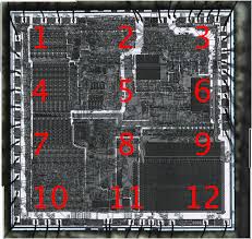
Crack Microcontroller dsPIC30F6014A Code
The oscillator start-up circuitry is not linked to the POR circuitry. Some crystal circuits (especially low frequency crystals) will have a relatively long start-up time. Therefore, one or more of the following conditions is possible after the POR timer and the PWRT have expired:
· The oscillator circuit has not begun to oscillate.
· The Oscillator Start-up Timer has NOT expired (if a crystal oscillator is used).
· The PLL has not achieved a LOCK (if PLL is used).
If the FSCM is disabled and the Power-up Timer (PWRT) is also disabled, then the device will exit rapidly from Reset on power-up. If the clock source is FRC, LPRC, EXTRC or EC, it will be active immediately. If the FSCM is disabled and the system clock has not started, the device will be in a frozen state at the Reset vector until the system clock starts. From the user’s perspective, the device will appear to be in Reset until a system clock is available.
A BOR will generate a Reset pulse which will reset the device. The BOR will select the clock source, based on the device Configuration bit values (FOS<2:0> and FPR<4:0>). Furthermore, if an oscillator mode is selected, the BOR will activate the Oscillator Start-up Timer (OST). The system clock is held until OST expires. If the PLL is used, then the clock will be held until the LOCK bit (OSCCON<5>) is ‘1’.
The primary function of the Watchdog Timer (WDT) is to reset the processor in the event of a software malfunction. The WDT is a free running timer, which runs off an on-chip RC oscillator, requiring no external component. Therefore, the WDT timer will continue to operate even if the main processor clock (e.g., the crystal oscillator) fails.
There are two power-saving states that can be entered through the execution of a special instruction, PWRSAV. These are: Sleep and Idle. The format of the PWRSAV instruction is as follows:
PWRSAV <parameter>, where ‘parameter’ defines Idle or Sleep mode.
The Watchdog Timer can be “Enabled” or “Disabled” only through a Configuration bit (FWDTEN) in the Configuration register FWDT. Setting FWDTEN = 1 enables the Watchdog Timer. The enabling is done when programming the device. By default, after chip-erase, FWDTEN bit = 1. Any device programmer capable of programming dsPIC30F devices allows programming of this and other Configuration bits.
If enabled, the WDT will increment until it overflows or “times out”. A WDT time-out will force a device Reset (except during Sleep). To prevent a WDT time-out, the user must clear the Watchdog Timer using a CLRWDT instruction.
If a WDT times out during Sleep, the device will wake up. The WDTO bit in the RCON register will be cleared to indicate a wake-up resulting from a WDT time-out. Setting FWDTEN = 0 allows user software to enable/disable the Watchdog Timer via the SWDTEN WDT time-out.
In Sleep mode, the clock to the CPU and peripherals is shutdown. If an on-chip oscillator is being used, it is shutdown. The Fail-Safe Clock Monitor is not functional during Sleep, since there is no clock to monitor. However, LPRC clock remains active if WDT is operational during Sleep.
The Brown-out protection circuit, if enabled, will remain functional during Sleep. The processor wakes up from Sleep if at least one of the following conditions has occurred:
· any interrupt that is individually enabled and meets the required priority level
· any Reset (POR, BOR and MCLR)
On waking up from Sleep mode, the processor will restart the same clock that was active prior to entry into Sleep mode. When clock switching is enabled, bits COSC<2:0> will determine the oscillator source that will be used on wake-up. If clock switch is disabled, then there is only one system clock.
The Low-Voltage Detect (LVD) module is used to detect when the VDD of the device drops below a threshold value, VLVD, which is determined by the LVDL<3:0> bits (RCON<11:8>) and is thus user programmable. The internal voltage reference circuitry requires a nominal amount of time to stabilize, and the BGST bit (RCON<13>) indicates when the voltage reference has stabilized if Crack Microcontroller.
In some devices, the LVD threshold voltage may be applied externally on the LVDIN pin. The LVD module is enabled by setting the LVDEN bit (RCON<12>).
Tags: Crack Microcontroller embedded archive,Crack Microcontroller embedded code,Crack Microcontroller embedded content,Crack Microcontroller embedded data,Crack Microcontroller embedded eeprom,Crack Microcontroller embedded file,crack microcontroller embedded firmware,Crack Microcontroller embedded information,crack microcontroller embedded memory,Crack Microcontroller embedded program