-
Product Categories
Live Support Chat


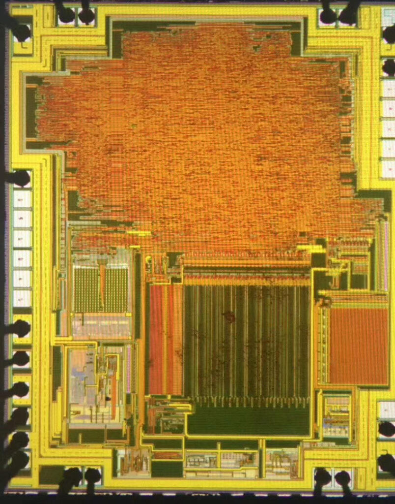
Crack Microcontroller ATmega128PV Heximal
Crack Microcontroller ATmega128PV and recover chip atmega128pv flash content in the format of Heximal, embedded program will be extracted from mcu atmega128pv memory;
Port 1 also receives the low-order address bytes during Flash programming and verification.
Port 2
Port 2 is an 8-bit bidirectional I/O port with internal pullups. The Port 2 output buffers can sink/source four TTL inputs. When 1s are written to Port 2 pins, they are pulled high by the internal pullups and can be used as inputs.
As inputs, Port 2 pins that are externally being pulled low will source current (IIL) because of the internal pullups. Port 2 emits the high-order address byte during fetches from external program memory and during accesses to external data memory that use 16-bit addresses (MOVX @ DPTR) if unlock attiny45 Microcontroller heximal.
In this application, Port 2 uses strong internal pullups when emitting 1s. During accesses to external data memory that use 8-bit addresses (MOVX @ RI), Port 2 emits the contents of the P2 Special Function Register.
Port 2 also receives the high-order address bits and some control signals during Flash programming and verification.
Port 3
Port 3 is an 8 bit bidirectional I/O port with internal pullups. The Port 3 output buffers can sink/source four TTL inputs. When 1s are written to Port 3 pins, they are pulled high by the internal pullups and can be used as inputs after unlock attiny85 Microcontroller heximal.
As inputs, Port 3 pins that are externally being pulled low will source current (IIL) because of the pullups. Port 3 also serves the functions of various special features of the AT89S53, as shown in the following table. Port 3 also receives some control signals for Flash programming and verification.
RST
Reset input. A high on this pin for two machine cycles while the oscillator is running resets the device.
ALE/PROG
Address Latch Enable is an output pulse for latching the low byte of the address during accesses to external memory. This pin is also the program pulse input (PROG) during Flash programming.
In normal operation, ALE is emitted at a constant rate of 1/6 the oscillator frequency and may be used for external timing or clocking purposes. Note, however, that one ALE pulse is skipped during each access to external data memory before unlock attiny2313a Microcontroller heximal.
Tags: crack processor archive,crack processor binary data,crack processor binary file,crack processor binary memory,crack processor code,crack processor content,crack processor eeprom,crack processor firmware,crack processor information,crack processor program