-
Product Categories
Live Support Chat


Crack Microcontroller ATmega1284 Heximal
Crack Microcontroller ATmega1284 Heximal of Flash and eeprom memory, extract the content out from its locked memory and copy the firmware to blank Microcontroller:
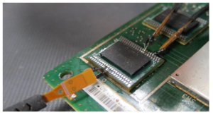
Crack Microcontroller ATmega1284 Heximal
The ATmega1284 features a 10-bit successive approximation ADC. The ADC is connected to a 4-channel Analog Multiplexer that allows one differential voltage input and four single-ended voltage inputs constructed from the pins of Port B.
The differential input (PB3, PB4) is equipped with a programmable gain stage, providing amplification step of 26 dB (20x) on the differential input voltage before the A/D conversion.
The single-ended voltage inputs at PB2..PB5 refer to 0V (GND). The ADC contains a Sample and Hold Amplifier that ensures that the input voltage to the ADC is held at a constant level during conversion.
A block diagram of the ADC is shown in Figure 25. An internal reference voltage of nominally 2.56V is provided On-chip and this reference can optionally be externally decoupled at the AREF (PB0) pin by a capacitor for better noise performance.
Alternatively, VCC can be used as reference voltage for single-ended channels. There is also an option to use an external voltage reference and turn off the internal voltage reference and traditional method for MCU reading.
These options are selected using the REFS1..0 bits of the ADMUX control register. The ADC converts an analog input voltage to a 10-bit digital value through successive approximation.
The minimum value represents GND and the maximum value represents the selected reference voltage minus 1 LSB. The voltage reference for the ADC may be selected by writing to the REFS1..0 bits in ADMUX.
VCC, the AREF pin, or an internal 2.56V reference may be selected as the ADC voltage reference. Optionally, the 2.56V internal voltage reference may be decoupled by an external capacitor at the AREF pin to improve noise immunity.
The analog input channel and differential gain are selected by writing to the MUX2..0 bits in ADMUX. Any of the four ADC input pins ADC3..0 can be selected as singleended inputs to the ADC.
ADC2 and ADC3 can be selected as positive and negative input, respectively, to the differential gain amplifier.
If differential channels are selected, the differential gain stage amplifies the voltage difference between the selected input pair by the selected gain factor, 1x or 20x, according to the setting of the MUX2..0 bits in ADMUX. This amplified value then becomes the analog input to the ADC. If single-ended channels are used, the gain amplifier is bypassed altogether.
Tags: crack microcontroller locked archive,crack microcontroller locked code,crack microcontroller locked content,crack microcontroller locked data,crack microcontroller locked eeprom,crack microcontroller locked file,crack microcontroller locked firmware,crack microcontroller locked information,crack microcontroller locked memory,crack microcontroller locked program
