-
Product Categories
Live Support Chat


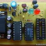
Crack Microcontroller AT89LS8252 Code
Crack Microcontroller AT89LS8252 and extract locked code from mcu at89ls8252 flash memory, the heximal content can be fully recovered from embedded mcu;
Features
Compatible with MCS-51™Products
8K Bytes of In-System Reprogrammable Downloadable Flash Memory
– SPI Serial Interface for Program Downloading
– Endurance: 1,000 Write/Erase Cycles 2K Bytes EEPROM
– Endurance: 100,000 Write/Erase Cycles
2.7V to 6V Operating Range
Fully Static Operation: 0 Hz to 12 MHz
Three-Level Program Memory Lock
256 x 8 bit Internal RAM
32 Programmable I/O Lines
Three 16 bit Timer/Counters
Nine Interrupt Sources
Programmable UART Serial Channel
SPI Serial Interface
Low Power Idle and Power Down Modes
Interrupt Recovery From Power Down
Programmable Watchdog Timer if read pic16f887 Microcontroller program
Dual Data Pointer
Power Off Flag
Description
The AT89LS8252 is a low-power, wide-voltage range, high-performance CMOS 8-bit microcomputer with 8K bytes of Downloadable Flash programmable and erasable read only memory and 2K bytes of EEPROM. The device is manufactured using Atmel’s high density nonvolatile memory technology and is compatible with the industry standard 80C51 instruction set and pinout.
The on-chip Downloadable Flash allows the program memory to be reprogrammed in-system through an SPI serial interface or by a conventional nonvolatile memory programmer. By combining a versatile 8-bit CPU with Downloadable Flash on a monolithic chip, the Atmel AT89LS8252 is a powerful microcomputer which provides a highly flexible and cost effective solution to many embedded control applications.
The AT89LS8252 provides the following standard features: 8K bytes of Downloadable Flash, 2K bytes of EEPROM, 256 bytes of RAM, 32 I/O lines, programmable watchdog timer, two Data Pointers, three 16-bit timer/counters, a six-vector two-level interrupt architecture, a full duplex serial port, on-chip oscillator, and clock circuitry.
In addition, the AT89LS8252 is designed with static logic for operation down to zero frequency and supports two software selectable power saving modes. The Idle Mode stops the CPU while allowing the RAM, timer/counters, serial port, and interrupt system to continue functioning. The Power Down Mode saves the RAM contents but freezes the oscillator, disabling all other chip functions until the next interrupt or hardware reset.
The Downloadable Flash can be changed a single byte at a time and is accessible through the SPI serial interface. Holding RESET active forces the SPI bus into a serial programming interface and allows the program memory to be written to or read from unless Lock Bit 2 has been activated.
Port 0 also receives the code bytes during Flash programming and outputs the code bytes during program verification. External pullups are required during program verification.
Port 1
Port 1 is an 8-bit bidirectional I/O port with internal pullups. The Port 1 output buffers can sink/source four TTL inputs. When 1s are written to Port 1 pins, they are pulled high by the internal pullups and can be used as inputs. As inputs, Port 1 pins that are externally being pulled low will source current (IIL) because of the internal pullups.
Some Port 1 pins provide additional functions. P1.0 and P1.1 can be configured to be the timer/counter 2 external count input (P1.0/T2) and the timer/counter 2 trigger input (P1.1/T2EX), respectively. Port 1 also receives the low-order address bytes during Flash programming and verification.
Port 2 is an 8-bit bidirectional I/O port with internal pullups. The Port 2 output buffers can sink/source four TTL inputs.When 1s are written to Port 2 pins, they are pulled high by the internal pullups and can be used as inputs. As inputs, Port 2 pins that are externally being pulled low will source current (IIL) because of the internal pullups.
Tags: crack microcontroller heximal archive,crack microcontroller heximal code,crack microcontroller heximal content,crack microcontroller heximal data,crack microcontroller heximal eeprom,crack microcontroller heximal file,crack microcontroller heximal firmware,crack microcontroller heximal information,crack microcontroller heximal memory,crack microcontroller heximal program