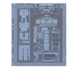
Crack MCU PIC18F8680 Binary
Crack MCU PIC18F8680 can disable the security fuse bits and extract the Binary or heximal out from memory include flash and eeprom, the code will be copied to other blank Microcontroller;
The PLL can only be enabled when the oscillator configuration bits are programmed for High-Speed Oscillator or External Clock mode. If they are programmed for any other mode, the PLL is not enabled and the system clock will come directly from OSC1.
There are two types of PLL modes: Software Controlled PLL and Configuration bits Controlled PLL. In Software Controlled PLL mode, PIC18F8680 executes at regular clock frequency after all Reset conditions. During execution, application can enable PLL and switch to 4x clock frequency operation by setting the PLLEN bit in the OSCCON register to faciliate the process of MCU Recovering.
In Configuration bits Controlled PLL mode, PIC18F8680 always executes with 4x clock frequency. The type of PLL is selected by programming the FOSC<3:0> configuration bits in the CONFIG1H Configuration register. The oscillator mode is specified during device programming.
A PLL lock timer is used to ensure that the PLL has locked before device execution starts. The PLL lock timer has a time-out that is called TPLL. The PIC18F8680 devices include a feature that allows the system clock source to be switched from the main oscillator to an alternate low-frequency clock source.
For the PIC18F8680 devices, this alternate clock source is the Timer1 oscillator. If a low-frequency crystal (32 kHz, for example) has been attached to the Timer1 oscillator pins and the Timer1 oscillator has been enabled, the device can switch to a low-power execution mode. The clock switching feature is enabled by programming the Oscillator Switching Enable (OSCSEN) bit in configuration register, CONFIG1H, to a ‘0’. Clock switching is disabled in an erased device.
The system clock source switching is performed under software control. The System Clock Switch bits, SCS1:SCS0 (OSCCON<1:0>), control the clock switching. When the SCS0 bit is ‘0’, the system clock source comes from the main oscillator that is selected by the FOSC configuration bits in configuration register, CONFIG1H. When the SCS0 bit is set, the system clock source will come from the Timer1 oscillator. The SCS0 bit is cleared on all forms of Reset.
When FOSC bits are programmed for software PLL mode, the SCS1 bit can be used to select between primary oscillator/clock and PLL output. The SCS1 bit will only have an effect on the system clock if the PLL is enabled (PLLEN =1) and locked (LOCK =1), else it will be forced clear. When programmed with Configuration Controlled PLL mode, the SCS1 bit will be forced clear.
Tags: crack mcu software archive,crack mcu software code,crack mcu software content,crack mcu software data,crack mcu software eeprom,crack mcu software file,crack mcu software firmware,crack mcu software information,crack mcu software memory,crack mcu software program


