Crack MCU PIC18F14K50 Heximal
Crack MCU PIC18F14K50 Heximal from its locked storage memory which include flash and eeprom, then copy the firmware like heximal or binary into blank Microcontroller;
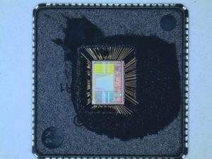
Crack MCU PIC18F14K50 Heximal
All of the devices in the PIC18F/LF1XK50 family offer ten different oscillator options, allowing users a wide range of choices in developing application hardware.
· Four Crystal modes, using crystals or ceramic resonators
· External Clock modes, offering the option of using two pins (oscillator input and a divide-by-4 clock output) or one pin (oscillator input, with the second pin reassigned as general I/O)
· External RC Oscillator modes with the same pin options as the External Clock modes
· An internal oscillator block which contains a 16 MHz HFINTOSC oscillator and a 31 kHz LFINTOSC oscillator which together provide 8 user selectable clock frequencies, from 31 kHz to 16 MHz. This option frees the two oscillator pins for use as additional general purpose I/O.
· A Phase Lock Loop (PLL) frequency multiplier, available to both the high-speed crystal and internal oscillator modes, which allows clock speeds of up to 48 MHz. Used with the internal oscillator, the PLL gives users a complete selection of clock speeds, from 31 kHz to 32 MHz – all without using an external crystal or clock circuit.
Besides its availability as a clock source, the internal oscillator block provides a stable reference source that gives the family additional features for robust operation:
· Fail-Safe Clock Monitor: This option constantly monitors the main clock source against a reference signal provided by the LFINTOSC. If a clock failure occurs, the controller is switched to the internal oscillator block, allowing for continued operation or a safe application shutdown.
· Two-Speed Start-up: This option allows the internal oscillator to serve as the clock source from Power-on Reset, or wake-up from Sleep mode, until the primary clock source is available.
· Memory Endurance: The Flash cells for both program memory and data EEPROM are rated to last for many thousands of erase/write cycles – up to 1K for program memory and 100K for EEPROM.
Data retention without refresh is conservatively estimated to be greater than 40 years.
· Self-programmability: These devices can write to their own program memory spaces under internal software control. Using a bootloader routine located in the code protected Boot Block, it is possible to create an application that can update itself in the field.
· Extended Instruction Set: The PIC18F/ LF1XK50 family introduces an optional extension to the PIC18 instruction set, which adds 8 new instructions and an Indexed Addressing mode. This extension has been specifically designed to optimize re-entrant application code originally developed in high-level languages, such as C.
· Enhanced CCP module: In PWM mode, this module provides 1, 2 or 4 modulated outputs for controlling half-bridge and full-bridge drivers. Other features include:
– Auto-Shutdown, for disabling PWM outputs on interrupt or other select conditions
– Auto-Restart, to reactivate outputs once the condition has cleared.
– Output steering to selectively enable one or more of 4 outputs to provide the PWM signal.
· Enhanced Addressable USART: This serial communication module is capable of standard RS-232 operation and provides support for the LIN bus protocol. Other enhancements include automatic baud rate detection and a 16-bit Baud Rate Generator for improved resolution.
· 10-bit A/D Converter: This module incorporates programmable acquisition time, allowing for a channel to be selected and a conversion to be initiated without waiting for a sampling period and thus, reduce code overhead.
· Extended Watchdog Timer (WDT): This enhanced version incorporates a 16-bit postscaler, allowing an extended time-out range that is stable across operating voltage and temperature.
Tags: crack mcu binary archive,crack mcu binary code,crack mcu binary content,crack mcu binary data,crack mcu binary eeprom,crack mcu binary file,crack mcu binary firmware,crack mcu binary information,crack mcu binary memory,crack mcu binary program
Related Products
-

Crack MCU PIC18LF14K50 Software
No. -

Crack MCU dsPIC30F4011 Binary
No. -

Crack MCU dsPIC30F3011 Program
No. -

Crack MCU dsPIC30F2012 Heximal
No. -

Crack MCU ATMEGA32PA Binary
No. -

Crack MCU ATMEGA16PA Heximal
No. -

Crack MCU ATMEGA8PA Binary
No. -

Crack MCU TS87C54X2 Heximal
No. -
Crack MCU TS87C51U2 Heximal
No. -

Crack MCU AT89C51AC3 Heximal
No.