-
Product Categories
Live Support Chat


Crack MCU dsPIC30F6011A Code
Crack MCU dsPIC30F6011A Code needs to disable the protection mechanism of microcontroller, through the modification on the circuitry pattern of Microcontroller through FIB technique will help to achieve this goal;
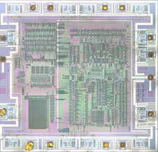
Crack MCU dsPIC30F6011A Code
Modified Harvard architecture
C compiler optimized instruction set architecture
Flexible addressing modes
84 base instructions
24-bit wide instructions, 16-bit wide data path
Up to 144 Kbytes on-chip Flash program space
Up to 48K instruction words
Up to 8 Kbytes of on-chip data RAM
· Up to 4 Kbytes of nonvolatile data EEPROM
· 16 x 16-bit working register array
· Up to 30 MIPs operation:
– DC to 40 MHz external clock input
– 4 MHz-10 MHz oscillator input with PLL active (4x, 8x, 16x)
· Up to 41 interrupt sources:
– 8 user selectable priority levels
– 5 external interrupt sources
– 4 processor traps
DSP Features:
· Dual data fetch
· Modulo and Bit-Reversed modes
· Two 40-bit wide accumulators with optional saturation logic
· 17-bit x 17-bit single-cycle hardware fractional/integer multiplier
· All DSP instructions are single cycle
– Multiply-Accumulate (MAC) operation
· Single-cycle ±16 shift
Peripheral Features:
· High-current sink/source I/O pins: 25 mA/25 mA
· Five 16-bit timers/counters; optionally pair up 16-bit timers into 32-bit timer modules
· 16-bit Capture input functions
· 16-bit Compare/PWM output functions:
· Data Converter Interface (DCI) supports common audio Codec protocols, including I2S and AC’97
· 3-wire SPI™ modules (supports 4 Frame modes)
· I2C™ module supports Multi-Master/Slave mode and 7-bit/10-bit addressing
· Two addressable UART modules with FIFO buffers
· Two CAN bus modules compliant with CAN 2.0B standard
Analog Features:
· 12-bit Analog-to-Digital Converter (ADC) with:
– 200 Ksps conversion rate
– Up to 16 input channels
– Conversion available during Sleep and Idle
· Programmable Low-Voltage Detection (PLVD)
· Programmable Brown-out Detection and Reset generation
Special Microcontroller Features:
· Enhanced Flash program memory:
– 10,000 erase/write cycle (min.) for industrial temperature range, 100K (typical)
· Data EEPROM memory:
– 100,000 erase/write cycle (min.) for industrial temperature range, 1M (typical)
· Self-reprogrammable under software control
· Power-on Reset (POR), Power-up Timer (PWRT) and Oscillator Start-up Timer (OST)
· Flexible Watchdog Timer (WDT) with on-chip low-power RC oscillator for reliable operation
Special Microcontroller Features (Cont.):
CMOS Technology:
· Fail-Safe Clock Monitor operation:
– Detects clock failure and switches to on-chip low-power RC oscillator
· Programmable code protection
Low-power, high-speed Flash technology
Wide operating voltage range (2.5V to 5.5V)
Industrial and Extended temperature ranges
Low power consumption
· In-Circuit Serial Programming™ (ICSP™)
· Selectable Power Management modes:
– Sleep, Idle and Alternate Clock modes if Crack MCU
The core has a 24-bit instruction word. The Program Counter (PC) is 23-bits wide with the Least Significant bit (LSb) always clear, and the Most Significant bit (MSb) is ignored during normal program execution, except for certain specialized instructions.
Thus, the PC can address up to 4M instruction words of user program space. An instruction prefetch mechanism is used to help maintain throughput. Program loop constructs, free from loop count management overhead, are supported using the DO and REPEAT instructions, both of which are interruptible at any point before Crack MCU.
The working register array consists of 16 x 16-bit registers, each of which can act as data, address or offset registers. One working register (W15) operates as a software Stack Pointer for interrupts and calls. The data space is 64 Kbytes (32K words) and is split into two blocks, referred to as X and Y data memory.
Each block has its own independent Address Generation Unit (AGU). Most instructions operate solely through the X memory, AGU, which provides the appearance of a single unified data space. The Multiply-Accumulate (MAC) class of dual source DSP instructions operate through both the X and Y AGUs, splitting the data address space into two parts. The X and Y data space boundary is device specific and cannot be altered by the user. Each data word consists of 2 bytes, and most instructions can address data either as words or bytes.
Tags: crack mcu heximal archive,crack mcu heximal code,crack mcu heximal content,crack mcu heximal data,crack mcu heximal eeprom,crack mcu heximal file,crack mcu heximal firmware,crack mcu heximal information,crack mcu heximal memory,crack mcu heximal program
Related Products
-

Crack MCU PIC18F45K22 Heximal
No. -

Crack MCU PIC18F43K22 Eeprom
No. -

Crack MCU dsPIC30F6010A Eeprom
No. -

Crack MCU dsPIC30F5015 Heximal
No. -

Crack MCU dsPIC30F5013 Firmware
No. -

Crack MCU PIC18F258 Software
No. -

Crack MCU ATMEGA168P Heximal
No. -

Crack MCU ATMEGA168A Heximal
No. -

Crack MCU ATMEGA128A Heximal
No. -

Crack MCU ATMEGA64PA Firmware
No.