-
Product Categories
Live Support Chat


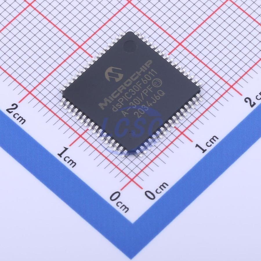
Crack MCU dsPIC30F6011 Heximal
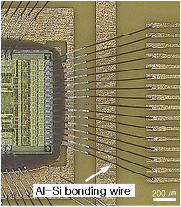
Crack MCU dsPIC30F6011 tamper resistance system and and extracted Heximal from locked microcontroller dsPIC30F6011 to recover the master MCU;
This document contains specific information for the dsPIC30F6011/6012/6013/6014 Digital Signal Controller (DSC) devices. The dsPIC30F devices contain extensive Digital Signal Processor (DSP) functionality within a high-performance 16-bit microcontroller (MCU) architecture. Figure 1-1 and Figure 1-2 show device block diagrams for dsPIC30F6011/6012 and dsPIC30F6013/6014 respectively.
This section contains a brief overview of the CPU architecture of the dsPIC30F. For additional hardware and programming information, please refer to the “dsPIC30F Family Reference Manual” (DS70046) and the “dsPIC30F/33F Programmer’s Reference Manual” (DS70157) respectively.
The core has a 24-bit instruction word. The Program Counter (PC) is 23 bits wide with the Least Significant bit (LSb) always clear (refer to Section 3.1 “Program Address Space”), and the Most Significant bit (MSb) is ignored during normal program execution, except for certain specialized instructions.
Thus, the PC can address up to 4M instruction words of user program space. An instruction prefetch mechanism is used to help maintain throughput. Program loop constructs, free from loop count management overhead, are supported using the DO and REPEAT instructions, both of which are interruptible at any point.
The working register array consists of 16 x 16-bit registers, each of which can act as data, address or offset registers. One working register (W15) operates as a software Stack Pointer for interrupts and calls. The data space is 64 Kbytes (32K words) and is split into two blocks, referred to as X and Y data memory.
Each block has its own independent Address Generation Unit (AGU). Most instructions operate solely through the X memory, AGU, which provides the appearance of a single unified data space. The Multiply-Accumulate (MAC) class of dual source DSP instructions operate through both the X and Y AGUs, splitting the data address space into two parts if Crack MCU.
(see Section 3.2 “Data Address Space”). The X and Y data space boundary is device specific and cannot be altered by the user. Each data word consists of 2 bytes, and most instructions can address data either as words or bytes.
There are two methods of accessing data stored in program memory:
The upper 32 Kbytes of data space memory can be mapped into the lower half (user space) of program space at any 16K program word boundary, defined by the 8-bit Program Space Visibility Page (PSVPAG) register. This lets any instruction access program space as if it were data space, with a limitation that the access requires an additional cycle. Moreover, only the lower 16 bits of each instruction word can be accessed using this method.
Linear indirect access of 32K word pages within program space is also possible using any working register, via table read and write instructions. Table read and write instructions can be used to access all 24 bits of an instruction word. Overhead-free circular buffers (Modulo Addressing) are supported in both X and Y address spaces. This is primarily intended to remove the loop overhead for DSP algorithms after Crack MCU.
The X AGU also supports Bit-Reversed Addressing on destination effective addresses to greatly simplify input or output data reordering for radix-2 FFT algorithms. Refer to Section 4.0 “Address Generator Units” for details on Modulo and Bit-Reversed Addressing. The core supports Inherent (no operand), Relative, Literal, Memory Direct, Register Direct, Register Indirect, Register Offset and Literal Offset Addressing modes.
Instructions are associated with predefined addressing modes, depending upon their functional requirements. For most instructions, the core is capable of executing a data (or program data) memory read, a working register (data) read, a data memory write and a program (instruction) memory read per instruction cycle.
As a result, 3-operand instructions are supported, allowing C = A + B operations to be executed in a single cycle. A DSP engine has been included to significantly enhance the core arithmetic capability and throughput. It features a high-speed 17-bit by 17-bit multiplier, a 40-bit ALU, two 40-bit saturating accumulators and a 40-bit bidirectional barrel shifter. Data in the accumulator or any working register can be shifted up to 15 bits right, or 16 bits left in a single cycle.
The DSP instructions operate seamlessly with all other instructions and have been designed for optimal real-time performance. The MAC class of instructions can concurrently fetch two data operands from memory while multiplying two W registers. To enable this concurrent fetching of data operands, the data space has been split for these instructions and linear for all others.
This has been achieved in a transparent and flexible manner, by dedicating certain working registers to each address space for the MAC class of instructions.
Tags: az MCU dsPIC30F6011 bináris program adatainak felújítása,az MCU dsPIC30F6011 bináris program adatainak helyreállítása,az MCU dsPIC30F6011 bináris program adatainak visszaállítása,fordított MCU dsPIC30F6011 bináris programadatok