-
Product Categories
Live Support Chat


Crack MCU dsPIC30F6010A Eeprom
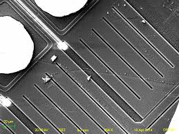
Crack MCU dsPIC30F6010A Eeprom starts from disable the security fuse bits of it and readout the firmware from the memory, the content will be same as the original Microcontroller;
Crack MCU dsPIC30F6010A Eeprom
High-Performance Modified RISC CPU:
· Modified Harvard architecture
· C compiler optimized instruction set architecture with flexible Addressing modes
· 83 base instructions
· 24-bit wide instructions, 16-bit wide data path
· 144 Kbytes on-chip Flash program space (Instruction words)
· 8 Kbytes of on-chip data RAM
· 4 Kbytes of nonvolatile data EEPROM
· Up to 30 MIPS operation:
– DC to 40 MHz external clock input
– 4 MHz-10 MHz oscillator input with PLL active (4x, 8x, 16x)
· 44 interrupt sources:
– 5 external interrupt sources
– 8 user selectable priority levels for each interrupt source
Dual data fetch
Accumulator write-back for DSP operations Modulo and Bit-Reversed Addressing modes Two, 40-bit wide accumulators with optional saturation logic
· 17-bit x 17-bit single-cycle hardware fractional/integer multiplier
· All DSP instructions single cycle
· ±16-bit single-cycle shift
Peripheral Features:
· High-current sink/source I/O pins: 25 mA/25 mA
· Timer module with programmable prescaler:
– Five 16-bit timers/counters; optionally pair 16-bit timers into 32-bit timer modules
· 16-bit Capture input functions
· 16-bit Compare/PWM output functions
· 3-wire SPI modules (supports 4 Frame modes)
· I2CTM module supports Multi-Master/Slave mode and 7-bit/10-bit addressing
· 2 UART modules with FIFO Buffers
· 2 CAN modules, 2.0B compliant (dsPIC306010A)
· 1 CAN module, 2.0B compliant (dsPIC306015)
The core has a 24-bit instruction word. The Program Counter (PC) is 23 bits wide with the Least Significant bit (LSb) always clear (see Section 3.1 “Program Address Space”), and the Most Significant bit (MSb) is ignored during normal program execution, except for certain specialized instructions. Thus, the PC can address up to 4M instruction words of user program space.
An instruction prefetch mechanism is used to help maintain throughput. Program loop constructs, free from loop count management overhead, are supported using the DO and REPEAT instructions, both of which are interruptible at any point.
The working register array consists of 16×16-bit registers, each of which can act as data, address or offset registers. One working register (W15) operates as a Software Stack Pointer for interrupts and calls for MCU code reading. The data space is 64 Kbytes (32K words) and is split into two blocks, referred to as X and Y data memory.
Each block has its own independent Address Generation Unit (AGU). Most instructions operate solely through the X memory AGU, which provides the appearance of a single unified data space. The Multiply-Accumulate (MAC) class of dual source DSP instructions operate through both the X and Y AGUs, splitting the data address space into two parts (see Section 3.2 “Data Address Space”).
The X and Y data space boundary is device-specific and cannot be altered by the user. Each data word consists of 2 bytes, and most instructions can address data either as words or bytes. There are two methods of accessing data stored in program memory.
Tags: crack mcu heximal archive,crack mcu heximal code,crack mcu heximal content,crack mcu heximal data,crack mcu heximal eeprom,crack mcu heximal file,crack mcu heximal firmware,crack mcu heximal information,crack mcu heximal memory,crack mcu heximal program
Related Products
-

Crack MCU PIC18F45K22 Heximal
No. -

Crack MCU PIC18F43K22 Eeprom
No. -

Crack MCU dsPIC30F6011A Code
No. -

Crack MCU dsPIC30F5015 Heximal
No. -

Crack MCU dsPIC30F5013 Firmware
No. -

Crack MCU PIC18F258 Software
No. -

Crack MCU ATMEGA168P Heximal
No. -

Crack MCU ATMEGA168A Heximal
No. -

Crack MCU ATMEGA128A Heximal
No. -

Crack MCU ATMEGA64PA Firmware
No.