-
Product Categories
Live Support Chat


Crack MCU dsPIC30F5015 Heximal
Crack MCU dsPIC30F5015 Heximal can copy the firmware of flash and eeprom memory, rewrite the program and data to blank Microcontroller to provide the same functions;
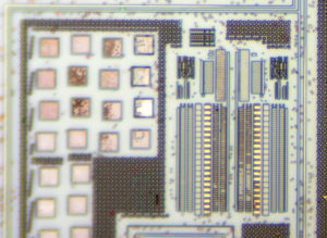
Crack MCU dsPIC30F5015 Heximal
High-Performance Modified RISC CPU:
· Modified Harvard architecture
· C compiler optimized instruction set architecture with flexible Addressing modes
· 83 base instructions
· 24-bit wide instructions, 16-bit wide data path
· 66 Kbytes on-chip Flash program space (Instruction words)
· 2 Kbytes of on-chip data RAM
· 1 Kbyte of nonvolatile data EEPROM
· Up to 30 MIPS operation:
– DC to 40 MHz external clock input
– 4 MHz-10 MHz oscillator input with PLL active (4x, 8x, 16x)
· 36 interrupt sources:
– Five external interrupt sources
– Eight user-selectable priority levels for each interrupt source
– Four processor trap sources
· 16 x 16-bit working register array
· Enhanced Flash program memory:
– 10,000 erase/write cycle (minimum) for industrial temperature range, 100K (typical)
· Data EEPROM memory:
– 100,000 erase/write cycle (minimum) for industrial temperature range, 1M (typical)
· Self-reprogrammable under software control
· Power-on Reset (POR), Power-up Timer (PWRT) and Oscillator Start-up Timer (OST)
· Flexible Watchdog Timer (WDT) with on-chip, low-power RC oscillator for reliable operation
· Fail-Safe Clock Monitor operation detects clock failure and switches to on-chip, low-power RC oscillator
· Programmable code protection
· In-Circuit Serial Programming™ (ICSP™) programming capability
– Sleep, Idle and Alternate Clock modes
This document contains device specific information for the dsPIC30F5015/5016 devices. The dsPIC30F devices contain extensive Digital Signal Processor (DSP) functionality within a high-performance 16-bit microcontroller (MCU) architecture.
Figure 1-1 is a block diagram of the dsPIC30F5015 device. Following the block diagram, Table 1-1 provides a brief description of the device I/O pinout and the functions that are multiplexed to the port pins on the dsPIC30F5015.
Figure 1-2 is a block diagram of the dsPIC30F5016 device. Following the block diagram, Table 1-2 provides a brief description of the device I/O pinout and the functions that are multiplexed to the port pins on the dsPIC30F5016.
Tags: crack mcu heximal archive,crack mcu heximal code,crack mcu heximal content,crack mcu heximal data,crack mcu heximal eeprom,crack mcu heximal file,crack mcu heximal firmware,crack mcu heximal information,crack mcu heximal memory,crack mcu heximal program
Related Products
-

Crack MCU PIC18F45K22 Heximal
No. -

Crack MCU PIC18F43K22 Eeprom
No. -

Crack MCU dsPIC30F6011A Code
No. -

Crack MCU dsPIC30F6010A Eeprom
No. -

Crack MCU dsPIC30F5013 Firmware
No. -

Crack MCU PIC18F258 Software
No. -

Crack MCU ATMEGA168P Heximal
No. -

Crack MCU ATMEGA168A Heximal
No. -

Crack MCU ATMEGA128A Heximal
No. -

Crack MCU ATMEGA64PA Firmware
No.