-
Product Categories
Live Support Chat


Crack MCU ATtiny26L Program
Crack MCU ATtiny26L and extract microcontroller ATtiny26L Program out from its flash memory and data from eeprom memory, copy the firmware to other blank Microcomputer for MCU cloning by recover its content;
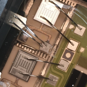
Crack MCU ATtiny26L and extract microcontroller ATtiny26L Program out from its flash memory and data from eeprom memory, copy the firmware to other blank Microcomputer for MCU cloning by recover its content;
The ATtiny26(L) provides 2K bytes of Flash, 128 bytes EEPROM, 128 bytes SRAM, up to 16 general purpose I/O lines, 32 general purpose working registers, two 8-bit Timer/Counters, one with PWM outputs, internal and external Oscillators, internal and external interrupts, programmable Watchdog Timer, 11-channel, 10-bit Analog to Digital Converter with two differential voltage input gain stages, and four software selectable power saving modes.
The Idle mode stops the CPU while allowing the Timer/Counters and interrupt system to continue functioning. The ATtiny26(L) also has a dedicated ADC Noise Reduction mode for reducing the noise in ADC conversion if Chip AT89C51RC binary unlocking.
In this sleep mode, only the ADC is functioning. The Power-down mode saves the register contents but freezes the oscillators, disabling all other chip functions until the next interrupt or hardware reset. The Standby mode is the same as the Power-down mode, but external oscillators are enabled.
The wakeup or interrupt on pin change features enable the ATtiny26(L) to be highly responsive to external events, still featuring the lowest power consumption while in the Power-down mode. The device is manufactured using Atmel’s high density non-volatile memory technology after MCU AT89C51ED2 flash unlocking.
By combining an enhanced RISC 8-bit CPU with Flash on a monolithic chip, the ATtiny26(L) is a powerful microcontroller that provides a highly flexible and cost effective solution to many embedded control applications. The ATtiny26(L) AVR is supported with a full suite of program and system development tools including: Macro assemblers, program debugger/simulators, In-circuit emulators, and evaluation kits.
AVCC is the supply voltage pin for Port A and the A/D Converter (ADC). It should be externally connected to VCC, even if the ADC is not used. If the ADC is used, it should be connected to VCC through a low-pass filter. See page 77 for details on operating of the ADC if Chip AT89C5130A flash unlocking.
Port B is an 8-bit general purpose I/O port. PB6..0 are all I/O pins that can provide internal pull-ups (selected for each bit). PB7 is an I/O pin if not used as the reset. To use pin PB7 as an I/O pin, instead of RESET pin, program (“0”) RSTDISBL Fuse. Port B has alternate functions for the ADC, clocking, timer counters, USI, SPI programming, and pin change interrupt as described in “Alternate Port Functions” on page 95. An External Reset is generated by a low level on the PB7/RESET pin. Reset pulses longer than 50 ns will generate a reset, even if the clock is not running. Shorter pulses are not guaranteed to generate a reset.
Tags: mcu protected archive crack,mcu protected code crack,mcu protected content crack,mcu protected data crack,mcu protected eeprom crack,mcu protected file crack,mcu protected firmware crack,mcu protected information crack,mcu protected memory crack,mcu protected program crack

