-
Product Categories
Live Support Chat


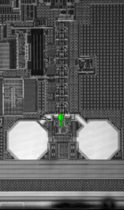
Crack MCU ATmega16PA Flash
Crack MCU ATmega16PA tamper resistance system and readout the content from its Flash and eeprom memory, copy the program and data to other blank Microcontroller;
Crack MCU ATmega16PA tamper resistance system and readout the content from its Flash and eeprom memory, copy the program and data to other blank Microcontroller
Port B is a 6-bit I/O port. PB4..0 are I/O pins that can provide internal pull-ups (selected for each bit). PB5 is input or open-drain output.
The use of pin PB5 is defined by a fuse and the special function associated with this pin is external Reset. The port pins are tristated when a reset condition becomes active, even if the clock is not running.
The internal oscillator provides a clock rate of nominally 1.6 MHz for the system clock (CK). Due to large initial variation (0.8 -1.6 MHz) of the internal oscillator, a tuning capability is built in.
Through an 8-bit control register – OSCCAL – the system clock rate can be tuned with less than 1% steps of the nominal clock.
There is an internal PLL that provides a 16x clock rate locked to the system clock (CK) for the use of the Peripheral Timer/Counter1. The nominal frequency of this peripheral clock, PCK, is 25.6 MHz.
The fast-access register file concept contains 32 x 8-bit general purpose working registers with a single-clock-cycle access time. This means that during one single clock cycle, one ALU (Arithmetic Logic Unit) operation is executed.
Two operands are output from the register file, the operation is executed, and the result is stored back in the register file – in one clock cycle.
Two of the 32 registers can be used as a 16-bit pointer for indirect memory access. This pointer is called the Z-pointer, and can address the register file, IO file and the Flash program memory.
The ALU supports arithmetic and logic functions between registers or between a constant and a register. Single-register operations are also executed in the ALU to faciliate Microcontroller memory copying process.
Figure 2 shows the ATtiny15L AVR RISC microcontroller architecture. The AVR uses a Harvard architecture concept with separate memories and buses for program and data memories.
The program memory is accessed with a two-stage pipeline. While one instruction is being executed, the next instruction is pre-fetched from the program memory.
This concept enables instructions to be executed in every clock cycle. The program memory is In-System Programmable Flash memory.
Tags: crack mcu protected archive,crack mcu protected bin,crack mcu protected code,crack mcu protected content,crack mcu protected data,crack mcu protected eeprom,crack mcu protected file,crack mcu protected firmware,crack mcu protected hex,crack mcu protected information,crack mcu protected memory,crack mcu protected program


