-
Product Categories
Live Support Chat


Crack MCU ATMEGA169V Flash
Crack MCU ATMEGA169V Flash and eeprom memory then extract IC code out from memory, replicate the program and data into other blank ATmega169V microcontroller for the same functions:
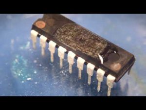
Crack MCU ATMEGA169V Flash and eeprom memory then extract IC code out from memory, replicate the program and data into other blank ATmega169V microcontroller for the same functions
In order to maximize performance and parallelism, the AVR uses a Harvard architecture – with separate memories and buses for program and data. Instructions in the program memory are executed with a single level pipelining. While one instruction is being executed, the next instruction is pre-fetched from the program memory.
This concept enables instructions to be executed in every clock cycle. The program memory is In-System Reprogrammable Flash memory. The fast-access Register File contains 32 x 8-bit general purpose working registers with a single clock cycle access time. This allows single-cycle Arithmetic Logic Unit (ALU) operation.
In a typical ALU operation, two operands are output from the Register File, the operation is executed, and the result is stored back in the Register File – in one clock cycle. Six of the 32 registers can be used as three 16-bit indirect address register pointers for Data Space addressing – enabling efficient address calculations before CPLD cracking.
One of the these address pointers can also be used as an address pointer for look up tables in Flash program memory. These added function registers are the 16-bit X-, Y-, and Z-register, described later in this section. The ALU supports arithmetic and logic operations between registers or between a constant and a register.
Single register operations can also be executed in the ALU. After an arithmetic operation, the Status Register is updated to reflect information about the result of the operation. Program flow is provided by conditional and unconditional jump and call instructions, able to directly address the whole address space.
Most AVR instructions have a single 16-bit word format. Every program memory address contains a 16- or 32-bit instruction. Program Flash memory space is divided in two sections, the Boot Program section and the Application Program section. Both sections have dedicated Lock bits for write and read/write protection.
The SPM instruction that writes into the Application Flash memory section must reside in the Boot Program section. During interrupts and subroutine calls, the return address Program Counter (PC) is stored on the Stack. The Stack is effectively allocated in the general data SRAM, and consequently the Stack size is only limited by the total SRAM size and the usage of the SRAM.
All user programs must initialize the SP in the Reset routine (before subroutines or interrupts are executed). The Stack Pointer (SP) is read/write accessible in the I/O space. The data SRAM can easily be accessed through the five different addressing modes supported in the AVR architecture.
Tags: mcu cracking locked archive,mcu cracking locked binary,mcu cracking locked code,mcu cracking locked content,mcu cracking locked data,mcu cracking locked eeprom,mcu cracking locked file,mcu cracking locked firmware,mcu cracking locked heximal,mcu cracking locked information,mcu cracking locked memory,mcu cracking locked program
