-
Product Categories
Live Support Chat


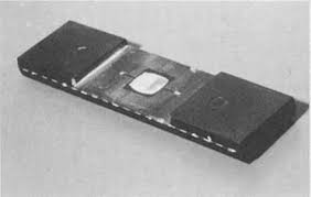
Crack MCU AT89C51CC03 Flash
Crack MCU AT89C51CC03 Flash memory start from reverse engineering microcontroller AT89C51CC03 to extract the circuitry scheme out from it, locate the security fuse bit of Microprocessor;
Crack MCU AT89C51CC03 Flash memory start from reverse engineering microcontroller AT89C51CC03 to extract the circuitry scheme out from it, locate the security fuse bit of Microprocessor
In a Master configuration, the SS line can be used in conjunction with the MODF flag in the SPI Status register (SPSCR) to prevent multiple masters from driving MOSI and SCK (see Error conditions). A high level on the SS pin puts the MISO line of a Slave SPI in a high-impedance state. The SS pin could be used as a general-purpose if the following conditions are met.
The device is configured as a Master and the SSDIS control bit in SPCON is set. This kind of configuration can be found when only one Master is driving the network and there is no way that the SS pin could be pulled low. Therefore, the MODF flag in the SPSCR will never be set(1). The Device is configured as a Slave with CPHA and SSDIS control bits set(2). This kind of configuration can happen when the system includes one Master and one Slave only. Therefore, the device should always be selected and there is no reason that the Master uses the SS pin to select the communicating Slave device.
Note:
Clearing SSDIS control bit does not clear MODF.
Special care should be taken not to set SSDIS control bit when CPHA =’0’ because in this mode, the SS is used to start the transmission.
In Master mode, the baud rate can be selected from a baud rate generator which is controlled by three bits in the SPCON register: SPR2, SPR1 and SPR0.The Master clock is selected from one of seven clock rates resulting from the division of the internal clock by 4, 8, 16, 32, 64 or 128 after Cracking Freescale Microprocessor MC9S12XDG128.
Table 90 gives the different clock rates selected by SPR2:SPR1:SPR0. In Slave mode, the maximum baud rate allowed on the SCK input is limited to Fsys/4 The Serial Peripheral Interface can be configured in one of the two modes: Master mode or Slave mode. The configuration and initialization of the SPI Module is made through two registers:
The Serial Peripheral Control register (SPCON)
The Serial Peripheral Status and Control Register (SPSCR)
Once the SPI is configured, the data exchange is made using:
The Serial Peripheral DATa register (SPDAT)
During an SPI transmission, data is simultaneously transmitted (shifted out serially) and received (shifted in serially). A serial clock line (SCK) synchronizes shifting and sampling on the two serial data lines (MOSI and MISO). A Slave Select line (SS) allows individual selection of a Slave SPI device; Slave devices that are not selected do not interfere with SPI bus activities.
The SPI operates in Master mode when the Master bit, MSTR (1), in the SPCON register is set. Only one Master SPI device can initiate transmissions. Software begins the transmission from a Master SPI Module by writing to the Serial Peripheral Data Register (SPDAT). If the shift register is empty, the Byte is immediately transferred to the shift register.
The Byte begins shifting out on MOSI pin under the control of the serial clock, SCK. Simultaneously, another Byte shifts in from the Slave on the Master’s MISO pin. The transmission ends when the Serial Peripheral transfer data flag, SPIF, in SPSCR becomes set. At the same time that SPIF becomes set, the received Byte from the Slaves transferred to the receive data register in SPDAT. Software clears SPIF by cracking the Serial Peripheral Status register (SPSCR) with the SPIF bit set, and then cracking the SPDAT before Microcontroller atmega48pa breaking.
The SPI operates in Slave mode when the Master bit, MSTR (2), in the SPCON register is cleared. Before a data transmission occurs, the Slave Select pin, SS, of the Slave device must be set to’0’. SS must remain low until the transmission is complete. In a Slave SPI Module, data enters the shift register under the control of the SCK from the Master SPI Module. After a Byte enters the shift register, it is immediately transferred to the receive data register in SPDAT, and the SPIF bit is set. To prevent an overflow condition, Slave software must then crack the SPDAT before another Byte enters the shift register (3). A Slave SPI must complete the write to the SPDAT (shift register) at least one bus cycle before the Master SPI starts a transmission. If the write to the data register is late, the SPI transmits the data alcracky in the shift register from the previous transmission.
Tags: crack mcu embedded archive,crack mcu embedded code,crack mcu embedded content,crack mcu embedded data,crack mcu embedded eeprom,crack mcu embedded file,crack mcu embedded firmware,crack mcu embedded information,crack mcu embedded memory,crack mcu embedded program
Related Products
-

Crack MCU PIC16F720 Binary
No. -

Crack MCU PIC18F4510 Firmware
No. -

Crack MCU ATTINY25 Heximal
No. -

Crack MCU ATTINY44 Firmware
No. -

Crack MCU ATTINY24V Program
No. -

Crack MCU AT89C51RB2 Eprom
No. -

Crack MCU AT89C51AC2 Software
No. -

Crack MCU AT89C51ID2 File
No. -

Crack MCU AT89C51CC03 Program
No. -

Crack MCU AT89C51AC3 Code
No.