-
Product Categories
Live Support Chat


Crack MCU AT89C51CC02 Code
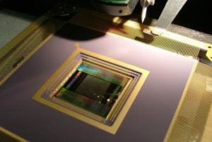
Crack MCU AT89C51CC02 and remove microcontroller’s security fuse bit, and recover microprocessor code from its flash and eeprom memory, replicate program and data to new MCU AT89C51CC02;
Crack MCU AT89C51CC02 and remove microcontroller’s security fuse bit, and recover microprocessor code from its flash and eeprom memory, replicate program and data to new MCU AT89C51CC02
The T89C51CC02 implements two general-purpose, 16-bit Timers/Counters. Such are identified as Timer 0 and Timer 1, and can be independently configured to operate in a variety of modes as a Timer or an event Counter. When operating as a Timer, the Timer/Counter runs for a programmed length of time, then issues an interrupt request.
When operating as a Counter, the Timer/Counter counts negative transitions on an external pin. After a preset number of counts, the Counter issues an interrupt request. The various operating modes of each Timer/Counter are described in the following sections if Microchip PIC18F4539 binary unlocking.
A basic operation is Timer registers THx and TLx (x = 0, 1) connected in cascade to form a 16-bit Timer. Setting the run control bit (TRx) in TCON register (See Figure 38) turns the Timer on by allowing the selected input to increment TLx. When TLx overflows it increments THx; when THx overflows it sets the Timer overflow flag (TFx) in TCON register.
Setting the TRx does not clear the THx and TLx Timer registers. Timer registers can be accessed to obtain the current count or to enter preset values. They can be read at any time but TRx bit must be cleared to preset their values, otherwise the behavior of the Timer/Counter is unpredictable after Reading MCU PIC18F4450 software.
The C/Tx# control bit selects Timer operation or Counter operation by selecting the divided-down peripheral clock or external pin Tx as the source for the counted signal. TRx bit must be cleared when changing the mode of operation, otherwise the behavior of the Timer/Counter is unpredictable.
For Timer operation (C/Tx# = 0), the Timer register counts the divided-down peripheral clock. The Timer register is incremented once every peripheral cycle (6 peripheral clock periods). The Timer clock rate is fPER/6, i.e. fOSC/12 in standard mode or fOSC/6 in X2 Mode when Chip PIC18F4455 eeprom reading.
For Counter operation (C/Tx# = 1), the Timer register counts the negative transitions on the Tx external input pin. The external input is sampled every peripheral cycles. When the sample is high in one cycle and low in the next one, the Counter is incremented. Since it takes 2 cycles (12 peripheral clock periods) to recognize a negative transition, the maximum count rate is fPER/12, i.e. fOSC/24 in standard mode or fOSC/12 in X2 Mode.
There are no restrictions on the duty cycle of the external input signal, but to ensure that a given level is sampled at least once before it changes, it should be held for at least one full peripheral cycle. Timer 0 functions as either a Timer or event Counter in four modes of operation.
Figure 24 through Figure 27 show the logical configuration of each mode. Timer 0 is controlled by the four lower bits of TMOD register (See Figure 39) and bits 0, 1, 4 and 5 of TCON register (See Figure 38). TMOD register selects the method of Timer gating (GATE0), Timer or Counter operation (T/C0#) and mode of operation (M10 and M00). TCON register provides Timer 0 control functions: overflow flag (TF0), run control bit (TR0), interrupt flag (IE0) and interrupt type control bit (IT0).
For normal Timer operation (GATE0 = 0), setting TR0 allows TL0 to be incremented by the selected input. Setting GATE0 and TR0 allows external pin INT0# to control Timer operation. Timer 0 overflow (count rolls over from all 1s to all 0s) sets TF0 flag generating an interrupt request.
It is important to stop Timer/Counter before changing mode. Mode 2 configures Timer 0 as an 8-bit Timer (TL0 register) that automatically reloads from TH0 register (See Figure 26). TL0 overflow sets TF0 flag in TCON register and reloads TL0 with the contents of TH0, which is preset by software. When the interrupt request is serviced, hardware clears TF0. The reload leaves TH0 unchanged.
The next reload value may be changed at any time by writing it to TH0 register. Mode 3 configures Timer 0 such that registers TL0 and TH0 operate as separate 8-bit Timers (See Figure 27). This mode is provided for applications requiring an additional 8-bit Timer or Counter. TL0 uses the Timer 0 control bits C/T0# and GATE0 in TMOD register, and TR0 and TF0 in TCON register in the normal manner.
TH0 is locked into a Timer function (counting FPER /6) and takes over use of the Timer 1 interrupt (TF1) and run control (TR1) bits. Thus, operation of Timer 1 is restricted when Timer 0 is in mode 3.
Tags: crack mcu flash archive,crack mcu flash code,crack mcu flash content,crack mcu flash data,crack mcu flash eeprom,crack mcu flash file,crack mcu flash firmware,crack mcu flash information,crack mcu flash memory,crack mcu flash program
Related Products
-
Crack Freescale MCU MC68HC705P6ACDW
No. -

Crack MCU PIC18F2458 Heximal
No. -

Crack MCU ATtiny261 Program
No. -

Crack MCU ATtiny4313 Binary
No. -

Crack MCU ATTINY85V Eeprom
No. -
Crack MCU PIC12F675 Binary
No. -

Crack MCU AT89C51RC2 Binary
No. -

Crack MCU AT89C51RD2 Eeprom
No. -

Crack MCU AT89C51RE2 Firmware
No. -

Crack MCU PIC18F85K90 Binary
No.