-
Product Categories
Live Support Chat


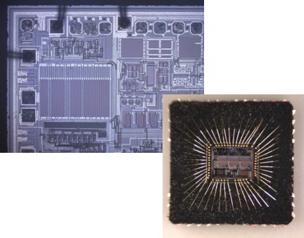
Crack MCU AT89C5131A Software
Crack MCU AT89C5131A needs to break microcontroller at89c5131a protection and extract embedded Software from mcu flash memory;
Introduction
The AT89C5130A/31A-M clock controller is based on an on-chip oscillator feeding an on-chip Phase Lock Loop (PLL). All the internal clocks to the peripherals and CPU core are generated by this controller.
The AT89C5130A/31A-M X1 and X2 pins are the input and the output of a single-stage on-chip inverter (see Figure 5-1) that can be configured with off-chip components as a Pierce oscillator (see Figure 5-2). Value of capacitors and crystal characteristics are detailed in the section “DC Characteristics” if read microcontroller pic16f876 flash.
The X1 pin can also be used as input for an external 48 MHz clock. The clock controller outputs three different clocks as shown in Figure 5-1:
a clock for the CPU core
a clock for the peripherals which is used to generate the Timers, PCA, WD, and Port sampling clocks
a clock for the USB controller
These clocks are enabled or disabled depending on the power reduction mode as detailed in Section “Power Management”, page 155.
The AT89C5130A/31A-M PLL is used to generate internal high frequency clock (the USB Clock) synchronized with an external low-frequency (the Peripheral Clock). The PLL clock is used to generate the USB interface clock. Figure 5-3 shows the internal structure of the PLL.
The PFLD block is the Phase Frequency Comparator and Lock Detector. This block makes the comparison between the reference clock coming from the N divider and the reverse clock coming from the R divider and generates some pulses on the Up or Down signal depending on the edge position of the reverse clock. The PLLEN bit in PLLCON register is used to enable the clock generation. When the PLL is locked, the bit PLOCK in PLLCON register (see Figure 5-3) is set.
The CHP block is the Charge Pump that generates the voltage reference for the VCO by injecting or extracting charges from the external filter connected on PLLF pin (see Figure 5-4). Value of the filter components are detailed in the Section “DC Characteristics”.
The VCO block is the Voltage Controlled Oscillator controlled by the voltage VREF produced by the charge pump. It generates a square wave signal: the PLL clock.
The Special Function Registers (SFRs) of the AT89C5130A/31A-M fall into the following categories:
C51 core registers: ACC, B, DPH, DPL, PSW, SP
I/O port registers: P0, P1, P2, P3, P4
Timer registers: T2CON, T2MOD, TCON, TH0, TH1, TH2, TMOD, TL0, TL1, TL2, RCAP2L, RCAP2H
Serial I/O port registers: SADDR, SADEN, SBUF, SCON
PCA (Programmable Counter Array) registers: CCON, CMOD, CCAPMx, CL, CH, CCAPxH, CCAPxL (x: 0 to 4)
Power and clock control registers: PCON
Hardware Watchdog Timer registers: WDTRST, WDTPRG
Interrupt system registers: IEN0, IPL0, IPH0, IEN1, IPL1, IPH1
Keyboard Interface registers: KBE, KBF, KBLS
LED register: LEDCON
Two Wire Interface (TWI) registers: SSCON, SSCS, SSDAT, SSADR
Serial Port Interface (SPI) registers: SPCON, SPSTA, SPDAT
USB registers: Uxxx (17 registers)
PLL registers: PLLCON, PLLDIV
BRG (Baud Rate Generator) registers: BRL, BDRCON
Flash register: FCON (FCON access is reserved for the Flash API and ISP software)
EEPROM register: EECON
Others: AUXR, AUXR1, CKCON0, CKCON1The AT89C5130A/31A-M implement 16/ 32 Kbytes of on-chip program/code memory. Figure 8-1 shows the split of internal and external program/code memory spaces depending on the product.
The Flash memory increases EPROM and ROM functionality by in-circuit electrical erasure and programming. Thanks to the internal charge pump, the high voltage needed for programming or erasing Flash cells is generated on-chip using the standard VDD voltage. Thus, the Flash Memory can be programmed using only one voltage and allows In-application Software Programming commonly known as IAP. Hardware programming mode is also available using specific programming tool.
The T89C5115 is a high performance Flash version of the 80C51 single chip 8-bit microcontrollers. It contains a 16-KB Flash memory block for program and data. The 16-KB Flash memory can be programmed either in parallel mode or in serial mode with the ISP capability or with software. The programming voltage is internally generated from the standard VCC pin.
The T89C5115 retains all features of the 80C52 with 256 bytes of internal RAM, a 7 source 4-level interrupt controller and three timer/counters. In addition, the T89C5115 has a 10-bit A/D converter, a 2-KB Boot Flash memory, 2-KB EEPROM for data, a Programmable Counter Array, an XRAM of 256 bytes, a Hardware WatchDog Timer and a more versatile serial channel that facilitates multiprocessor communication (EUART).
The fully static design of the T89C5115 reduces system power consumption by bringing the clock frequency down to any value, even DC, without loss of data. The T89C5115 has two software-selectable modes of reduced activity and an 8 bit clock prescaler for further reduction in power consumption. In the idle mode the CPU is frozen while the peripherals and the interrupt system are still operating. In the power-down mode the RAM is saved and all other functions are inoperative.
The added features of the T89C5115 make it more powerful for applications that need A/D conversion, pulse width modulation, high speed I/O and counting capabilities such as industrial control, consumer goods, alarms, motor control, etc. While remaining fully compatible with the 80C52 it offers a superset of this standard microcontroller.
In X2 mode a maximum external clock rate of 20 MHz reaches a 300 ns cycle time.
Port Structure
Each Port SFR operates via type-D latches, as illustrated in Figure 1 for Ports 3 and 4. A CPU ’write to latch’ signal initiates transfer of internal bus data into the type-D latch. A CPU ’read latch’ signal transfers the latched Q output onto the internal bus. Similarly, a ’read pin’ signal transfers the logical level of the Port pin. Some Port data instructions activate the ’read latch’ signal while others activate the ’read pin’ signal
Latch instructions are referred to as Read-Modify-Write instructions. Each I/O line may be independently programmed as input or output. Figure 1 shows the structure of Ports, which have internal pull-ups. An external source can pull the pin low. Each Port pin can be configured either for general-purpose I/O or for its alternate input output function.
To use a pin for general-purpose output, set or clear the corresponding bit in the Px register (x = 1 to 4). To use a pin for general-purpose input, set the bit in the Px register. This turns off the output FET drive. To configure a pin for its alternate function, set the bit in the Px register. When the latch is set, the ’alternate output function’ signal controls the output level (See Figure 1). The operation of Ports is discussed further in ’Quasi-Bi-directional Port Operation’ paragraph.
It is not obvious that the last three instructions in this list are Read-Modify-Write instructions. These instructions read the port (all 8 bits), modify the specifically addressed bit and write the new byte back to the latch. These Read-Modify-Write instructions are directed to the latch rather than the pin in order to avoid possible misinterpretation of voltage (and therefore, logic) levels at the pin.
For example, a Port bit used to drive the base of an external bipolar transistor cannot rise above the transistor’s base-emitter junction voltage (a value lower than VIL). With a logic one written to the bit, attempts by the CPU to read the Port at the pin are misinterpreted as logic zero. A read of the latch rather than the pins returns the correct logic one value.
Tags: crack mcu heximal archive,crack mcu heximal code,crack mcu heximal content,crack mcu heximal data,crack mcu heximal eeprom,crack mcu heximal file,crack mcu heximal firmware,crack mcu heximal information,crack mcu heximal memory,crack mcu heximal program
Related Products
-

Crack MCU PIC18F45K22 Heximal
No. -

Crack MCU PIC18F43K22 Eeprom
No. -

Crack MCU dsPIC30F6011A Code
No. -

Crack MCU dsPIC30F6010A Eeprom
No. -

Crack MCU dsPIC30F5015 Heximal
No. -

Crack MCU dsPIC30F5013 Firmware
No. -

Crack MCU PIC18F258 Software
No. -

Crack MCU ATMEGA168P Heximal
No. -

Crack MCU ATMEGA168A Heximal
No. -

Crack MCU ATMEGA128A Heximal
No.