-
Product Categories
Live Support Chat


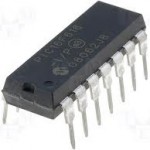
Crack IC PIC18LF14K22 Heximal
Crack IC PIC18LF14K22 Heximal is a process to unlock the status of Microcontroller PIC18LF14K22 and disable the security fuse bit, extract the embedded firmware out from its memory.
Crack IC PIC18LF14K22 Heximal
The programming block size is 8 or 16 bytes, depending on the device (See Table 4-1). Word or byte programming is not supported. Table writes are used internally to load the holding registers needed to program the Flash memory. There are only as many holding registers as there are bytes in a write block.
Since the Table Latch (TABLAT) is only a single byte, the TBLWT instruction may need to be executed 8, or 16 times, depending on the device, for each programming operation. All of the table write operations will essentially be short writes because only the holding registers are written.
After all the holding registers have been written, the programming operation of that block of memory is started by configuring the EECON1 register for a program memory write and performing the long write sequence.
The long write is necessary for programming the internal Flash. Instruction execution is halted during a long write cycle. The long write will be terminated by the internal programming timer. The EEPROM on-chip timer controls the write time. The write/erase voltages are generated by an on-chip charge pump, rated to operate over the voltage range of the device.
The data EEPROM is a nonvolatile memory array, separate from the data RAM and program memory, which is used for long-term storage of program data. It is not directly mapped in either the register file or program memory space but is indirectly addressed through the Special Function Registers (SFRs). The EEPROM is readable and writable during normal operation over the entire VDD range.
Four SFRs are used to read and write to the data EEPROM as well as the program memory. The data EEPROM allows byte read and write. When interfacing to the data memory block, EEDATA holds set and cleared when the internal programming timer expires and the write operation is complete.
The EEPROM data memory is rated for high erase/write cycle endurance. A byte write automatically erases the location and writes the new data (erase-before-write). The write time is controlled by an on-chip timer; it will vary with voltage and temperature as well as from chip-to-chip. Please refer to parameter US122.The EEADR register is used to address the data EEPROM for read and write operations. The 8-bit range of the register can address a memory range of 256 bytes (00h to FFh).
Access to the data EEPROM is controlled by two registers: EECON1 and EECON2. These are the same registers which control access to the program memory and are used in a similar manner for the data EEPROM. The EECON1 register (Register 5-1) is the control register for data and program memory access. Control bit EEPGD determines if the access will be to program or data EEPROM memory. When the EEPGD bit is clear, operations will access the data EEPROM memory.
When the EEPGD bit is set, program memory is accessed. Control bit, CFGS, determines if the access will be to the Configuration registers or to program memory/data EEPROM memory. When the CFGS bit is set, subsequent operations access Configuration registers. When the CFGS bit is clear, the EEPGD bit selects either program Flash or data EEPROM memory. The WREN bit, when set, will allow a write operation. On power-up, the WREN bit is clear. The WRERR bit is set by hardware when the WR bit is set and cleared when the internal programming timer expires and the write operation is complete.
Tags: crack ic binary archive,crack ic binary code,crack ic binary content,crack ic binary data,crack ic binary eeprom,crack ic binary file,crack ic binary firmware,crack ic binary information,crack ic binary memory,crack ic binary program