-
Product Categories
Live Support Chat


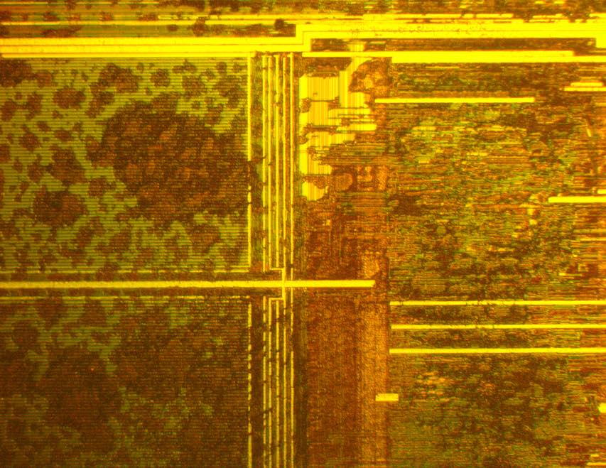
Crack IC PIC16F726 Eeprom
Crack IC PIC16F726 Eeprom and copy the embedded heximal from microcontroller pic16f726, the fuse bit of mcu will be attacked to removed the security protection;
The Special Function Registers are registers used by the CPU and peripheral functions for controlling the desired operation of the device (refer to Table 2-1). These registers are static RAM. The Special Function Registers can be classified into two sets: core and peripheral. The Special Function Registers associated with the “core” are described in this section.
Those related to the operation of the peripheral features are described in the section of that peripheral feature. The STATUS register, shown in Register 2-1, contains:
· the arithmetic status of the ALU
· the Reset status
· the bank select bits for data memory (SRAM)
The STATUS register can be the destination for any instruction, like any other register. If the STATUS register is the destination for an instruction that affects the Z, DC or C bits, then the write to these three bits is disabled. These bits are set or cleared according to the device logic.
Furthermore, the TO and PD bits are not writable. Therefore, the result of an instruction with the STATUS register as destination may be different than intended. The Program Counter (PC) is 13 bits wide. The low byte comes from the PCL register, which is a readable and writable register. The high byte (PC<12:8>) is not directly readable or writable and comes from PCLATH if restoring mcu sst89e58rd firmware.
On any Reset, the PC is cleared. Figure 2-7 All devices are capable of addressing a continuous 8K word block of program memory. The CALL and GOTO instructions provide only 11 bits of address to allow branching within any 2K program memory page. When doing a CALL or GOTO instruction, the upper 2 bits of the address are provided by PCLATH<4:3>.
In Compare mode, the 16-bit CCPRx register value is constantly compared against the TMR1 register pair value. When a match occurs, the CCPx module:
· Toggle the CCPx output
In Compare mode, Timer1 must be running in either Timer mode or Synchronized Counter mode. The compare operation may not work in Asynchronous Counter mode.
Set the CCPx output before Crack IC
Clear the CCPx output
Generate a Special Event Trigger
Generate a Software Interrupt after Crack IC
Note:
Clocking Timer1 from the system clock (FOSC) should not be used in Compare mode. For the Compare operation of the TMR1 register to the CCPRx register to occur, All Compare modes can generate an interrupt. The Compare Mode is dependent upon the system clock (FOSC) for proper operation. Since FOSC is shut down during Sleep mode, the Compare mode will not function properly during Sleep when Crack IC.
Tags: crack ic binary archive,crack ic binary code,crack ic binary content,crack ic binary data,crack ic binary eeprom,crack ic binary file,crack ic binary firmware,crack ic binary information,crack ic binary memory,crack ic binary program