-
Product Categories
Live Support Chat


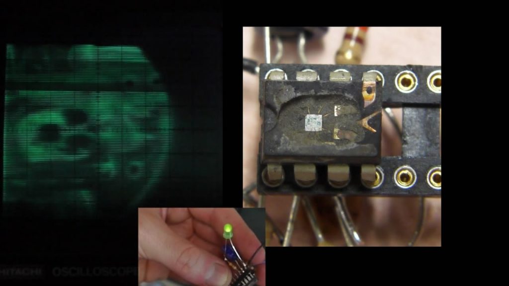
Crack Chip PIC18F87K90 Binary
Crack Chip PIC18F87K90 secured flash memory and readout MCU PIC18F87K90 Binary after reverse engineering PIC18F87K90 microcontroller in the reverse order of Integrated circuit technology;
The PGC and PGD pins are used for In-Circuit Serial Programming™ (ICSP™) and debugging purposes. It is recommended to keep the trace length between the ICSP connector and the ICSP pins on the device as short as possible. If the ICSP connector is expected to experience an ESD event, a series resistor is recommended, with the value in the range of a few tens of ohms, not to exceed 100Ω.
Pull-up resistors, series diodes and capacitors on the PGC and PGD pins are not recommended as they will interfere with the programmer/debugger communications to the device. If such discrete components are an application requirement, they should be removed from the circuit during programming and debugging if Crack microcontroller pic18f2553 bin.
Alternatively, refer to the AC/DC characteristics and timing requirements information in the respective device Flash programming specification for information on capacitive loading limits, and pin input voltage high (VIH) and input low (VIL) requirements.
For device emulation, ensure that the “Communication Channel Select” (i.e., PGCx/PGDx pins) programmed into the device matches the physical connections for the ICSP to the Microchip debugger/emulator tool. For more information on available Microchip development tools connection requirements, refer to Section 30.0 “Development Support” after extract ic pic18f4553 program.
Many microcontrollers have options for at least two oscillators: a high-frequency primary oscillator and a low-frequency secondary oscillator (refer to Section 3.0 “Oscillator Configurations” for details). The oscillator circuit should be placed on the same side of the board as the device.
Place the oscillator circuit close to the respective oscillator pins with no more than 0.5 inch (12 mm) between the circuit components and the pins. The load capacitors should be placed next to the oscillator itself, on the same side of the board.
Use a grounded copper pour around the oscillator circuit to isolate it from surrounding circuits. The grounded copper pour should be routed directly to the MCU ground. Do not run any signal traces or power traces inside the ground pour. Also, if using a two-sided board, avoid any traces on the other side of the board where the crystal is placed.
Layout suggestions are shown in Figure 2-4. In-line packages may be handled with a single-sided layout that completely encompasses the oscillator pins. With fine-pitch packages, it is not always possible to completely surround the pins and components when Crack MCU memory.
A suitable solution is to tie the broken guard sections to a mirrored ground layer. In all cases, the guard trace(s) must be returned to ground. In planning the application’s routing and I/O assignments, ensure that adjacent port pins and other signals in close proximity to the oscillator are benign (i.e., free of high frequencies, short rise and fall times, and other similar noise).
Tags: crack chip binary archive,crack chip binary code,crack chip binary content,crack chip binary data,crack chip binary eeprom,crack chip binary file,crack chip binary firmware,crack chip binary information,crack chip binary memory,crack chip binary program


