-
Product Categories
Live Support Chat


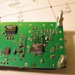
Crack Chip PIC18F4610 Heximal
Crack Chip PIC18F4610 starts from disable the protective mechamism of microcontroller PIC18F4610 and readout the Heximal from the flash and eeprom memory, then replicate the code to blank MCU which provide the same functions as original MCU;

Crack Chip PIC18F4610 starts from disable the protective mechamism of microcontroller PIC18F4610 and readout the Heximal from the flash and eeprom memory, then replicate the code to blank MCU which provide the same functions as original MCU
When PRI_IDLE mode is selected, the designated primary oscillator continues to run without interruption. For all other power managed modes, the oscillator using the OSC1 pin is disabled. The OSC1 pin (and OSC2 pin, if used by the oscillator) will stop oscillating.
In secondary clock modes (SEC_RUN and SEC_IDLE), the Timer1 oscillator is operating and providing the device clock. The Timer1 oscillator may also run in all power managed modes if required to clock Timer1 or Timer3.
In internal oscillator modes (RC_RUN and RC_IDLE), the internal oscillator block provides the device clock source. The 31 kHz INTRC output can be used directly to provide the clock and may be enabled to support various special features, regardless of the power managed mode.
The INTOSC output at 8 MHz may be used directly to clock the device or may be divided down by the postscaler. The INTOSC output is disabled if the clock is provided directly from the INTRC output. If the Sleep mode is selected, all clock sources are stopped. Since all the transistor switching currents have been stopped, Sleep mode achieves the lowest current consumption of the device (only leakage currents) by extract IC code.
Enabling any on-chip feature that will operate during Sleep will increase the current consumed during Sleep. The INTRC is required to support WDT operation. The Timer1 oscillator may be operating to support a real-time clock. Other features may be operating that do not require a device clock source (i.e., SSP slave, PSP, INTn pins and others). Peripherals that may add significant current consumption are listed.
Power-up delays are controlled by two timers, so that no external Reset circuitry is required for most applications. The delays ensure that the device is kept in Reset until the device power supply is stable under normal circumstances and the primary clock is operating and stable. For additional information on power-up delays.
The first timer is the Power-up Timer (PWRT), which provides a fixed delay on power-up (parameter 33, Table 25-10). It is enabled by clearing (= 0) the PWRTEN configuration bit.
Tags: crack chip embedded archive,crack chip embedded code,crack chip embedded content,crack chip embedded data,crack chip embedded eeprom,crack chip embedded file,crack chip embedded firmware,crack chip embedded information,crack chip embedded memory,crack chip embedded program