Crack Chip PIC16F723 Software
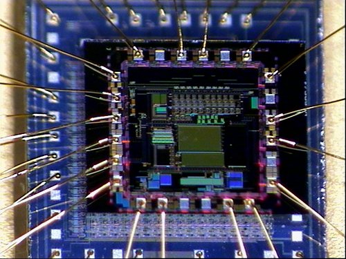
Crack Chip PIC16F723 fuse bit and extract IC code from embedded flash memory, internal structure of microcontroller flash memory will be reverse engineered to discover the location of fuse bit;

The PIC16F72X/PIC16LF72X has a noise filter in the MCLR Reset path. The filter will detect and ignore small pulses. It should be noted that a Reset does not drive the MCLR pin low. Voltages applied to the pin that exceed its specification can result in both MCLR Resets and excessive current beyond the device specification during the ESD
For this reason, Microchip recommends that the MCLR pin no longer be tied directly to VDD. The use of an RC network, as shown in Figure 3-2, is suggested. An internal MCLR option is enabled by clearing the MCLRE bit in the Configuration Word register. When MCLRE = 0, the Reset signal to the chip is generated internally when break microchip mcu pic16lf877.
When the MCLRE = 1, the RE3/MCLR pin becomes an external Reset input. In this mode, the RE3/MCLR pin has a weak pull-up to VDD. In-Circuit Serial Programming is not affected by selecting the internal MCLR option. The Power-up Timer provides a fixed 64 ms (nominal) time-out on power-up only, from POR or Brown-out Reset.
The Power-up Timer operates from the WDT oscillator. For more information, see Section 7.3 “Internal Clock Modes”. The chip is kept in Reset as long as PWRT is active. The PWRT delay allows the VDD to rise to an acceptable level. A Configuration bit, PWRTE, can disable (if set) or enable (if cleared or programmed) the Power-up Timer. The Power-up Timer should be enabled when Brown-out Reset is enabled, although it is not required after extract cpld xilinx xc95144 jed file.
The Power-up Timer delay will vary from chip-to-chip and vary due to:
· VDD variation
· Temperature variation
· Process variation
The on-chip POR circuit holds the chip in Reset until VDD has reached a high enough level for proper operation. A maximum rise time for VDD is required. See Section 23.0 “Electrical Specifications” for details. If the BOR is enabled, the maximum rise time specification does not apply. The BOR circuitry will keep the device in Reset until VDD reaches VBOR (see Section 3.5 “Brown-Out Reset (BOR)”) after extract ti dsp mcu tms320f2812.
When the device starts normal operation (exits the Reset condition), device operating parameters (i.e., voltage, frequency, temperature, etc.) must be met to ensure operation. If these conditions are not met, the device must be held in Reset until the operating conditions are met.
For additional information, refer to Application Note AN607, “Power-up Trouble Shooting” (DS00607). Brown-out Reset is enabled by programming the BOREN<1:0> bits in the Configuration register. The brown-out trip point is selectable from two trip points via the BORV bit in the Configuration register. Between the POR and BOR, complete voltage range coverage for execution protection can be implemented.
Two bits are used to enable the BOR. When BOREN = 11, the BOR is always enabled. When BOREN = 10, the BOR is enabled, but disabled during Sleep. When BOREN = 0X, the BOR is disabled. If VDD falls below VBOR for greater than parameter (TBOR) (see Section 23.0 “Electrical Specifications”), the Brown-out situation will reset the device.
This will occur regardless of VDD slew rate. A Reset is not ensured to occur if VDD falls below VBOR for more than parameter (TBOR). If VDD drops below VBOR while the Power-up Timer is running, the chip will go back into a Brown-out Reset and the Power-up Timer will be re-initialized.
Once VDD rises above VBOR, the Power-up Timer will execute a 64 ms Reset. On power-up, the time-out sequence is as follows: first, PWRT time-out is invoked after POR has expired, then OST is activated after the PWRT time-out has expired. The total time-out will vary based on oscillator configuration and PWRTE bit status. For example, in EC mode with PWRTE bit = 1 (PWRT disabled), there will be no time-out at all. Figure 3-4, Figure 3-5 and Figure 3-6 depict time-out sequences.
Since the time-outs occur from the POR pulse, if MCLR is kept low long enough, the time-outs will expire. Then, bringing MCLR high will begin execution immediately (see Figure 3-5). This is useful for testing purposes or to synchronize more than one PIC16F72X/PIC16LF72X device operating in parallel. Table 3-3 shows the Reset conditions for some special registers.
Tags: crack chip flash archive,crack chip flash code,crack chip flash content,crack chip flash data,crack chip flash eeprom,crack chip flash file,crack chip flash firmware,crack chip flash information,crack chip flash memory,crack chip flash program


