-
Product Categories
Live Support Chat


Clone TMS320F28023 MCU Flash Program
The flash control mode register is located at I/O address FF0Fh which is also the importat address to Clone TMS320F28023 MCU Flash Program. This register offers two options: register access mode and array access mode. Register access mode gives access to the four control registers in the memory space decoded for the flash module.
These registers are used to control erasing, programming, and testing of the flash array. Register access mode is enabled by activating an OUT command with dummy data only after the completion of Locked IC PIC18F2220 Code Cracking.
The OUT xxxx, FF0Fh instruction makes the flash registers accessible for reads and/or writes. After executing OUT xxxx, FF0Fh, the flash control registers are accessed in the memory space decoded for the flash module and the flash array cannot be accessed. The four registers are repeated every four address locations within the flash module’s decoded range through the process of Restore MCU microchip SST89E58RD2A.
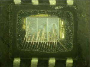
Clone TMS320F28023 MCU Flash Program
After completing all the necessary reads and/or writes to the control registers, an IN xxxx, FF0Fh instruction (with dummy data) is executed to place the flash array back in array access mode in order to Crack Protected MC68HC08AZ60 Memory. After executing the IN xxxx, FF0Fh instruction, the flash array is accessed in the decoded space and the flash registers are not available.
Switching between the register access mode and the array access mode is done by issuing the IN and OUT instructions. The memory content in these instructions (denoted by xxxx) is not relevant. Refer to the TMS320F28023 DSPs Embedded Flash Memory Technical Reference (literature number SPRU282) for a detailed description of the flash programming algorithms when Break IC.