-
Product Categories
Live Support Chat


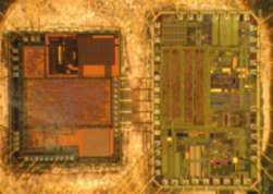
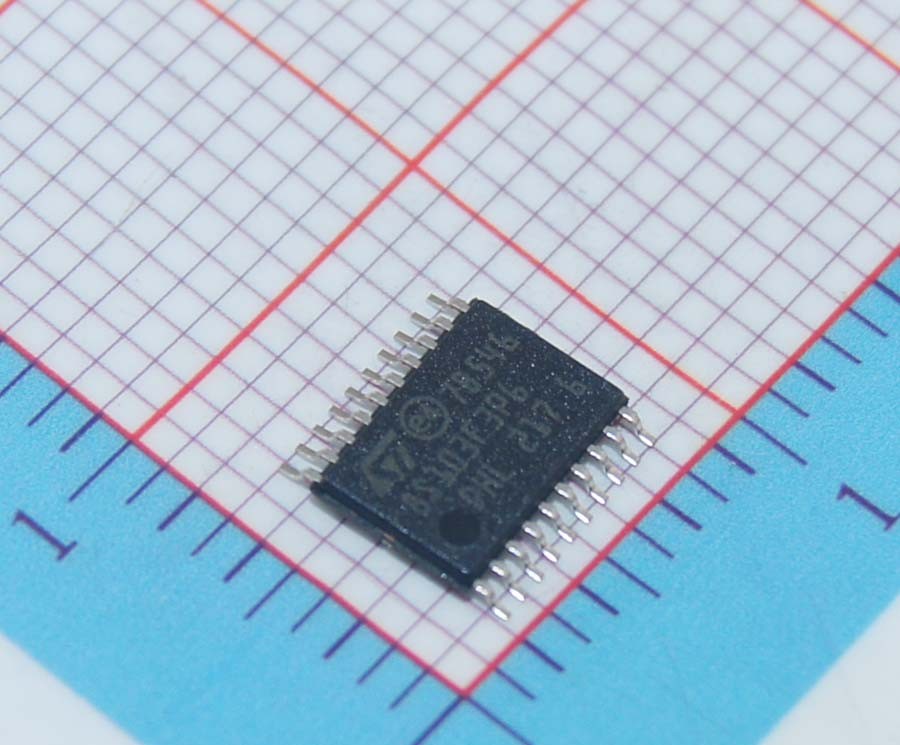
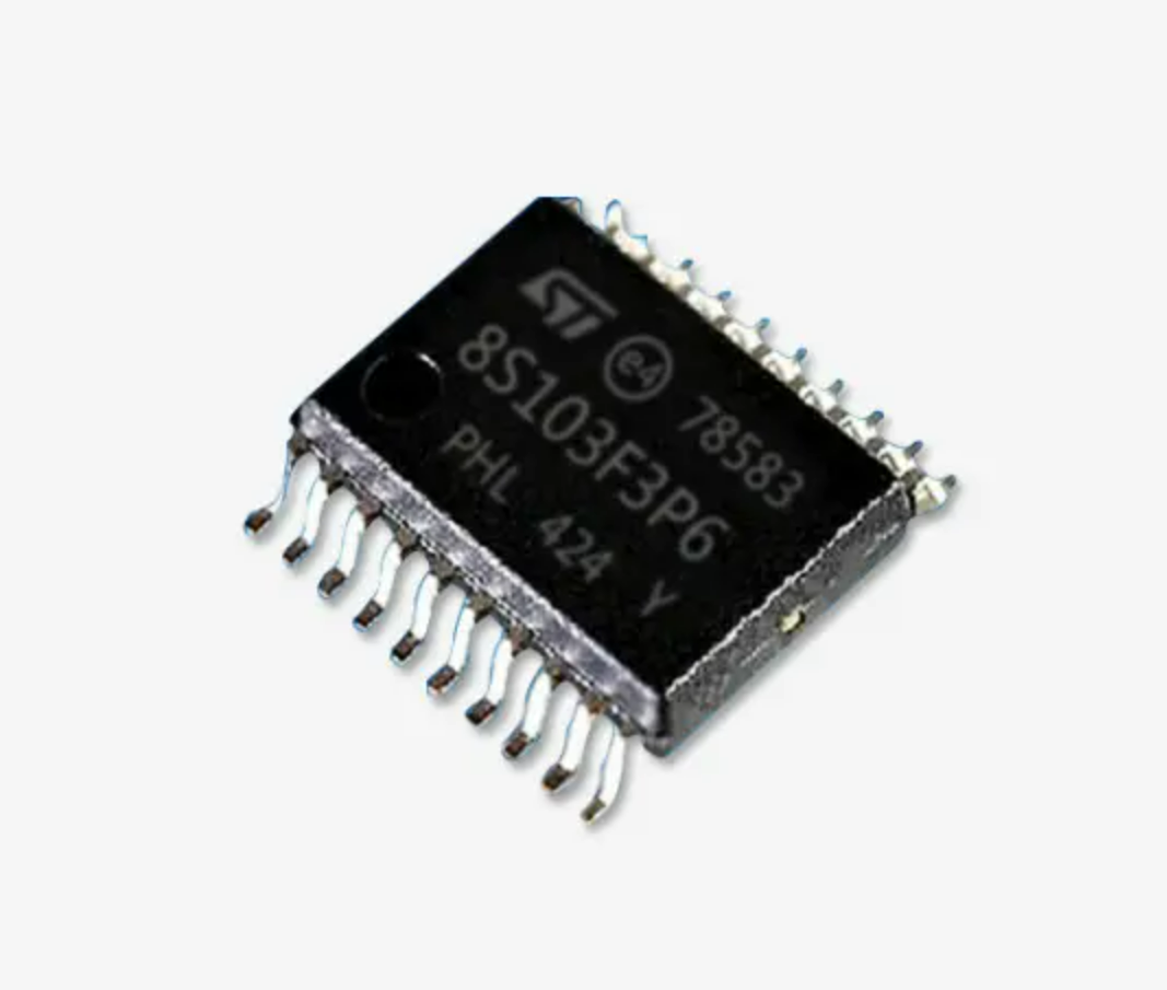
Clone STM8S103F3P3 MCU Chip Locked Program Code
Clone STM8S103F3P3 MCU Chip Locked Program Code needs to break off stm8s103f3p3 cpu flash memory’s fuse bit and extract heximal code from mcu stm8s103f3p3 flash memory;
Analog-to-digital converter (ADC1)
STM8S003F3/K3 value line products contain a 10-bit successive approximation A/D converter (ADC1) with up to 5 external multiplexed input channels and the following main features:
Input voltage range: 0 to VDDA
Conversion time: 14 clock cycles
Single and continuous, buffered continuous conversion modes
Buffer size (10 x 10 bits)
Scan mode for single and continuous conversion of a sequence of channels to unlock stm8s103f3p6 flash memory;
Analog watchdog capability with programmable upper and lower thresholds
Analog watchdog interrupt
External trigger input
Trigger from TIM1 TRGO
End of conversion (EOC) interrupt
Note: Additional AIN12 analog input is not selectable in ADC scan mode or with analog watchdog.
Values converted from AIN12 are stored only into the ADC_DRH/ADC_DRL registers.
Communication interfaces
The following communication interfaces are implemented:
UART1: full feature UART, synchronous mode, SPI master mode, SmartCard mode, IrDA mode, LIN2.1 master capability when clone stm8s105k4 flash code;
SPI: full and half-duplex, 8 Mbit/s
I²C: up to 400 Kbit/s