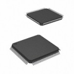
Clone MCU ATTINY461A Code
Clone MCU ATTINY461A Code and reprogramme the firmware to other blank Microcontroller ATtiny461A which will provide the same functions as original MCU, MCU program reading can effectively help engineer to recover the lost data from eeprom and program from flash;
Clone MCU ATTINY461A Code and reprogramme the firmware to other blank Microcontroller ATtiny461A which will provide the same functions as original MCU, MCU program reading can effectively help engineer to recover the lost data from eeprom and program from flash
The EEPROM Programming mode bit setting defines which programming action that will be triggered when writing EEPE. It is possible to program data in one atomic operation (erase the old value and program the new value) or to split the Erase and Write operations in two different operations.
The Programming times for the different modes are shown in Table 2. While EEPE is set, any write to EEPMn will be ignored. During reset, the EEPMn bits will be reset to 0b00 unless the EEPROM is busy programming when extract microcontroller pic12f617 binary.
Writing EERIE to one enables the EEPROM Ready Interrupt if the I bit in SREG is set. Writing EERIE to zero disables the interrupt. The EEPROM Ready interrupt generates a constant interrupt when EEPE is cleared.
The EEMPE bit determines whether setting EEPE to one causes the EEPROM to be written. When EEMPE is set, setting EEPE within four clock cycles will write data to the EEPROM at the selected address If EEMPE is zero, setting EEPE will have no effect.
When EEMPE has been written to one by software, hardware clears the bit to zero after four clock cycles. See the description of the EEPE bit for an EEPROM write procedure after unlock pic12hv615 heximal.
The EEPROM Write Enable Signal EEPE is the write strobe to the EEPROM. When address and data are correctly set up, the EEPE bit must be written to one to write the value into the EEPROM. The EEMPE bit must be written to one before a logical one is written to EEPE, otherwise no EEPROM write takes place.
The following procedure should be followed when writing the EEPROM (the order of steps 3 and 4 is not essential):
- Wait until EEPE becomes zero.
- Wait until SELFPRGEN in SPMCSR becomes zero.
- Write new EEPROM address to EEAR (optional).
- Write new EEPROM data to EEDR (optional).
- Write a logical one to the EEMPE bit while writing a zero to EEPE in EECR if clone mcu code.
- Within four clock cycles after setting EEMPE, write a logical one to EEPE.
The EEPROM can not be programmed during a CPU write to the Flash memory. The software must check that the Flash programming is completed before initiating a new EEPROM write. Step 2 is only relevant if the software contains a Boot Loader allowing the CPU to program the Flash. If the Flash is never being updated by the CPU, step 2 can be omitted. See “Memory Programming” on page 335 for details about Boot programming.
Tags: clone mcu archive,clone mcu bin,clone mcu code,clone mcu content,clone mcu data,clone mcu eeprom,clone mcu file,clone mcu firmware,clone mcu hex,clone mcu information,clone mcu memory,clone mcu program